D'Oh! Attached is a pic of the 2 I am still wrestling w/.Two of the red ones are 220pF. Four are 100pF.

For those future builders who won't be buying from the power supply Group Buy, here is the Mouser cart I put together when helping with the project documentation earlier.
You can edit it without affecting the master cart.
https://www.mouser.com/ProjectManager/ProjectDetail.aspx?AccessID=d80094b24f
Please note the following:
1. As of this post, all parts in the cart are in stock.
2. There are 5 options for filter caps C6-11 in the BOM in the Build Guide. I've included every one of these, but you will need to delete the one(s) you don't want to order, or you'll get a lot of different filter caps and run up your cost! Refer to the Customer # column for information.
3. There are two transformer options in the BOM. Mouser only carries the 12V option; if you want to use the Talema, order it from Digikey and delete the Signal from your Mouser cart.
4. Select the proper voltage fuse for your mains voltage and delete the other.
As people are starting to get their kits, here's the guide, which will help greatly with parts identification.
This is still very under construction, so hang in there and reload the guide often. It's not quite ACA level, but is pretty detailed, as this is not a simple project.
Take your time, read everything, print out the build doc.
https://guides.diyaudio.com/Guide/Pearl+3/28
This is still very under construction, so hang in there and reload the guide often. It's not quite ACA level, but is pretty detailed, as this is not a simple project.
Take your time, read everything, print out the build doc.
https://guides.diyaudio.com/Guide/Pearl+3/28
The infamous ZVP3310 in Pearl Two that was known to die in assembly if you looked at it sideways is one of the things that was designed out of Pearl 3.
There are no parts that are particularly sensitive, just use normal handling.
There are no parts that are particularly sensitive, just use normal handling.
Last edited:
Only at low frequencies. Above few kHz cartrige L blocks shunting.The 47k input resistor is shunted by a low impedance -- the cartridge.
@6L6 Love you man! I was wondering about the guide about 2 hrs. ago, outstanding job, but we wouldn't expect less!
Thanks for all your continued efforts to support the community & Happy New Year To All!
Thanks for all your continued efforts to support the community & Happy New Year To All!
Had a couple of new OPA1656, so mounted them to DIP adapters and will likely try them tomorrow.
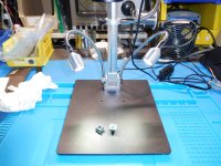
@ktf7 - SMD takes some practice, but if you use a good iron, good quality solder, water-soluble flux paste, and good visors or magnifier, it will come quickly to you. I've used mostly a visor but recently bought a nice USB microscope that helps with really small stuff.
@ktf7 - SMD takes some practice, but if you use a good iron, good quality solder, water-soluble flux paste, and good visors or magnifier, it will come quickly to you. I've used mostly a visor but recently bought a nice USB microscope that helps with really small stuff.
Attachments
I'm afraid to ask, my head might explode, but here goes. I assume static is the culprit, but what makes 1 so sensitive vs another?The infamous ZVP3310 in Pearl Two that was known to die in assembly if you looked at it sideways
The ZVP3310 is a P-channel mosfet. Mos have the lowest breakdown voltage, from what I understand. Hopefully somebody who actually knows the answer can jump in.
I haven't had any problems at all with the transistors in the kit, in this project or in any other applications.
I haven't had any problems at all with the transistors in the kit, in this project or in any other applications.
Last edited:
The "O" in MOSFET is oxide. That's the insulator which separates the Gate terminal from the conducting channel from Source to Drain.
Fabs make the insulator thin because that reduces the distance from Gate to channel. Which means in layman's terms the Gate has more "control" over the channel, i.e., the gain is higher. People want amplifying devices with loads of gain.
However, thin insulators break down at low applied voltage, while thick insulators break down at high applied voltage. The thin silicon dioxide in a modern MOSFET, breaks down (destroying the MOSFET!!!) at less than 50 volts. That's why MOSFET datasheets specify an ABSOLUTE MAXIMUM gate-to-source voltage which is usually 20 volts or less.
As you may suspect, when a human being shuffles her feet on a thick pile carpet and then touches something metallic, the painful electric spark that occurs is a discharge of MUCH MORE than 50 volts. Executive Summary: Human Body Electrostatic Discharge Kills MOSFETs.
Solution 1: handle MOSFETs very very carefully. (Perl 2). Solution 2: leave MOSFETs out of your design. (Perl 3)
Source: have personally designed and built MOSFETs since 1978. Just like many other Forum members.
Last edited:
- Home
- Amplifiers
- Pass Labs
- Pearl 3 Burning Amp 2023