
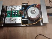
At the end this is a monoblock intended as test equipment in my lab. With exceptional performance, no rf-residues typical for class-D .. and rock solid.
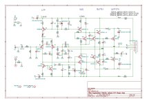
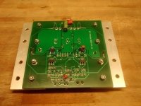
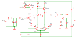
Q14 and Q15 ??The next step was the pcb-layout based on KiCAD.
Try this one. You can change the frequency amplitude and rise time of the input signal in the circled command.
Thanks, that makes it a lot easier!
Also had some time this weekend to play with you schematic. Replaced the R3 with a constant current source, as @WhiteDragon suggested. Decreased the input impedance to 10k and input sensitivity to about 1V, with makes more sense to me.Had to change R9 (a lot from 12 k to 2k7 in order to get the DC balance right). Adjusted the current through the VAS transistors to about 6 mA by decreasing R4 and R5.
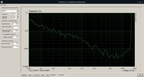
Managed to get the distortion down to 0,0004 % at 1 khz 1w into 8 ohms. It increases to about 0,02 % at 1 kHz. The input RC-network seems to have great impact of the square wave response. Higher value of C1 drops the slew rate and also increases distortion at high frequencies a lot. To small and there to much ringing I think. Settled at 1000pF and added inductor at the output. Drops slew rate to about 24v/µS, but looks ok I think.
Thinking of building a board for this one to see if it's actually working.
What I don't really understand with this circuit is that how the VAS is working. I guess R8, R11, D1 are forming some sort of current regulator for the differential pair of TR3 and TR4?
Attachments
Looks good 🙂 Its a very tweakable circuit.
Although it looks like a differential pair it doesn't quite behave like one. You can actually remove TR3 and it all works but the slew rate isn't quite as good. R8, D1 and TR5 are a conventional current source. R8 and D1 generate a fixed voltage across them (although it isn't that constant with changes in supply voltage) and R11 sets the current.
A two resistor bootstrapped current source might be worth investigating.

What I don't really understand with this circuit is that how the VAS is working. I guess R8, R11, D1 are forming some sort of current regulator for the differential pair of TR3 and TR4?
Although it looks like a differential pair it doesn't quite behave like one. You can actually remove TR3 and it all works but the slew rate isn't quite as good. R8, D1 and TR5 are a conventional current source. R8 and D1 generate a fixed voltage across them (although it isn't that constant with changes in supply voltage) and R11 sets the current.
A two resistor bootstrapped current source might be worth investigating.
Aha, so if R8 and D1 is used for reference voltage for TR5, i thought I could use the reference voltage from the base of Q1 instead. I did work, but I had to rise the current for the VAS by decreasing R11 some, from 6 to 8mA in order to restore the DC balance. Though I don't think this it did any improvement. Slew rate actually dropped a bit and distortion at 20 kHz increased slightly.

Still can't understand the reason for R9 and C6 in the circuit, and why it affects the DC balance so much.
Tried without TR3 and it was much better with TR3.
Bootstrapped current source? Can you elaborate that?
Still can't understand the reason for R9 and C6 in the circuit, and why it affects the DC balance so much.
Tried without TR3 and it was much better with TR3.
A two resistor bootstrapped current source might be worth investigating.
Bootstrapped current source? Can you elaborate that?
Still can't understand the reason for R9 and C6 in the circuit, and why it affects the DC balance so much.
Glad your having fun.
Over the years have always come back to this
topology.
Referring to schematic in post #28
Seems like you found most the tricks to getting
current/ and offset right.
I to in the beginning lowered R9 for offset.
But have found the positive side will rail stick
when clipping with sinewave if too low value.
And found higher values usually needed for good performance.
usually min 10k to 12k like original.
As noticed TR3/ TR4 best performance is 6ma to 7ma
no higher or lower.
Once below 6ma or above 7ma you will notice THD
and performance will drop.
And the circuit really wakes up when dialed in.
Noticed same thing with R4/R5 values.
Used to dial in TR3/TR4 current levels.
But have found best performance no lower
than 2.7K but I use 30 volt rails for sim.
DC offset is the only frustrating thing usually.
With non inverting. DC Offset I keep positive.
And I too like very low offset.
But usually accept 1 to 2mv.
If your having trouble with offset but currents
are ideal.
Just like original have found R2 will be slightly higher
than R7 feedback resistor.
And then play with the Current source current to get offset set.
Technically around 2ma no higher. but can go as low as 1.5ma
to dial in offset. You would with conventional knowledge think
slew rate would be better at higher current. But as long
as its 1.5 to 2ma to get offset dialed in.
Performance stays the same.
You only see big performance jumps if R4/R5 are too high
or too low. and have found 2.7k usually lowest threshold.
and 3.9k as original is highest threshold.
also have seen C5 sometimes not needed and can reduce ringing.
But if needed to make high frequency ringing go down.
Can be a much lower value than C6
C5 can be around 3.3p to 5.6p if needed.
Also can increase C4 to 10n to help stabilize and it
wont effect slew rate.
Otherwise as noted C5 can be removed sometimes
and will reduce ringing. If needed , value set lower
than C6
Little quirks with the circuit. Main point
I usually leave R9 at high value 10k to 12k
for no rail stick. And dial in offset further
with current source 1.5 to 2ma and make
R2 slightly higher for about 1 to 2mv positive offset.
About all you get. Non inverting should be positive.
I use Tina TI and also find in sim.
Device temps should be set to at least 20c
and I set Vas to 25c and outputs to 45c
to get a more realistic idea of what real world
DC offset would be. If everything is too cold.
DC offset not as realistic
Last edited:
Aha, so if R8 and D1 is used for reference voltage for TR5, i thought I could use the reference voltage from the base of Q1 instead
Q1's reference voltage is always going to be low at 0.6v across R3. You could try removing Q2 and using an LED (say green for a couple of volts drop) to set the base to plus rail voltage). You would then need to increase R3 to maintain your 2ma constant current to the input pair.
Now use that higher LED reference voltage for TR5.
Looking at the original sim (my-/+45 volt rails) and R9 can even be shorted with no real change apart from throwing more dissipation onto TR3 although it is still under 0.5 watt. I've never seen an original explanation that I recall detailing how and why it was done that way.Still can't understand the reason for R9 and C6 in the circuit, and why it affects the DC balance so much.
Q1's reference voltage is always going to be low at 0.6v across R3. You could try removing Q2 and using an LED (say green for a couple of volts drop) to set the base to plus rail voltage). You would then need to increase R3 to maintain your 2ma constant current to the input pair.
Now use that higher LED reference voltage for TR5.
Think I see what you mean. Using a LED as voltage reference for both the input and VAS CCS I got it working with a few parts less. Unfortunately the distortion increased to 0,0009 %. Still acceptable I guess and a lot less parts.
I still don't understand what R9 does, and why it has to be connected the base of TR5.
I to in the beginning lowered R9 for offset.
But have found the positive side will rail stick
when clipping with sinewave if too low value.
And found higher values usually needed for good performance.
usually min 10k to 12k like original.
Ok, did see that, why R9 could be as low. But I manage redesign the schematic, keeping the R9 higher at 10k. Performance is about the same as before. 0,0004 % THD at 1W 1khz.
Getting rid of C5 was I good idea. Now I can use a lower values for C1, like 100 pF, without to much ringing (keeping the inductor at 1µH). This also lowers the distortion at 20khz to only 0,01%.
Tempering with R2/R7 ratio in order to adjust the offset seems really tricky btw. Slightest change in resistance ratio affects the DC offset very much. Maybe this could be problem in a real design. But I could always use a pot to dial the offset I guess.
I was thinking of using a current mirror as well. Since the use of a CCS lowered the distortion it could benefit from that. Tried putting a current mirror before R4 and R5, but never got it working. Had to add some degeneration resistor to make it stable, but could see any improvements actually. However this is beyond me knowledge really...
Attachments
Oh no, man, do not build such an input stage in noninverting config.
It have too much common mode error vs common mode itself due to the Early's effect.
At least put a cascode for current source and main long tailed pair transistors.
It have too much common mode error vs common mode itself due to the Early's effect.
At least put a cascode for current source and main long tailed pair transistors.
At least put a cascode for current source and main long tailed pair transistors.
What do you mean with cascode? Like a current mirror?
A cascode current source on the long-tailed pair will decouple the rail ripple much better than a simple current source, so long as the cascode is decoupled to ground. This eliminates the Early effect on the current source.
H
HAYK
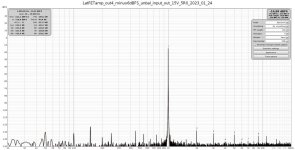
You are measuring wrong the distortion. In post 28 I get 0.00038% 1w 1khz and 0.0053% 20khz.
You need to let 10 cycles before start saving data for only one cycle.
Short the output inductors.
You need to let 10 cycles before start saving data for only one cycle.
Short the output inductors.
Are you talking about R9 and C4?Still can't understand the reason for R9 and C6 in the circuit,
R9 is present to equalize the power dissipation of the TR3 and TR4 differential pair. When connected directly to the current mirror input (cathode of D1) without R9, TR3 generates about twice as much heat as TR4. Therefore, an output offset drift occurs from the time the power is turned on until the temperature of the transistor pair reaches equilibrium. Therefore, set this resistor to a value so that the collector potentials of TR3 and TR4 are approximately equal.
However, this resistor creates a mirror effect on Q4 and prevents Q4's collector current from being accurately transferred to the input of the high-side current mirror. (Loss increases at high frequencies) To compensate for this, C4 is inserted in parallel with R9. This value should be sufficiently larger than C5 (including Cob of Tr3) to suppress the influence of the mirror effect of TR3. Specifically, 10 times or more is sufficient.
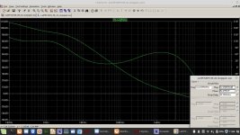
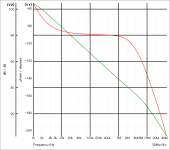
Below is a comparative simulation with and without C4 = 6.8n.
In order to see the open loop characteristics up to VAS, the output stage was replaced with an ideal buffer and the feedback circuit was also changed.
Also, since the input filter is also an obstacle, we set C2=0 and measure the characteristics before the output inductor.
In order to match the collector voltages of Tr3 and Tr4, R9 is set to 3.9k. (Results from my simulation)
Since this circuit is a 1-pole phase compensation, it is desired that high frequencies be attenuated by -6dB/octave and the phase shift should be -90°.
Green is gain and red is phase sift. The solid line is C4 = 6.8n, and the dotted line is without C4.
There is also a method of adding a cascode Tr(Q3 in the circuit below) to Tr4 instead of these RCs.
This also has a straightforward open loop characteristic, similar to the with C4 in the graph above.
Attachments
Last edited:
And it's base to the cascode of Tr4 for keeping potentials around secand LTP's collectors nearly the same.of adding a cascode Tr(Q3 in the circuit below)
Also Tr4 collector needs stabilizing load to the ground, say 1MOhm for excluding board leaks, fingerprints and flux washing issues.
- Home
- Amplifiers
- Solid State
- VAS requirements for MOSFET OPS