Stef,
C7 outer foil should be connected to opamp output.
When designing pcb use ground plane on top and bottom, at least around opamp and input.
Voltages measured are ok.
While testing, I suggest you to use a max. 3A fuse on output. This for short-cut protection. Later on, you may increase this to a fast 10A fuse.
Regards,
Tibi
Last edited by a moderator:
Yes, this may be a fast solution.The OpAmp is missing the required LPF RC on the input !
A carefully designed PCB with groundplane or signal guard, may be an elegant solution.
Regards,
Tibi
Hello Tibi,
Ground plane on both side is problematic to manage. Superimposed and uncontrolled ground planes can create parasitic capacitances and induce losses in the bandwidth of the device.
What is a "signal guard"?
Regards,
Stef.
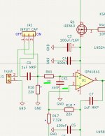
ps : C7 is connected as needed. If I reverse C7, the output offset is a bit higher. I put a "*" on the silkcreen to indicate the direction.
Ground plane on both side is problematic to manage. Superimposed and uncontrolled ground planes can create parasitic capacitances and induce losses in the bandwidth of the device.
What is a "signal guard"?
Regards,
Stef.
ps : C7 is connected as needed. If I reverse C7, the output offset is a bit higher. I put a "*" on the silkcreen to indicate the direction.
Last edited:
There is a LPF after opamp that limit amplifier BW at ~125KHz.
I do not use input LPF because internal cabling and PCB layout can eliminate any EMI. Cabling matter, pcb layout mater a lot.
If you want to "secure" input opamp I would go for a LPF at 1MHz. For this use 1K5 with 100pF.
Lately, I spent some time, to design a PCB with dual ground plane on input section. This ensure signal guarding as well. Two mosfet pairs, rounded traces, castelated holes etc.
I'll update github documents with this version and other things in the next weeks.
Regards,
Tibi
After.
Also, before input capacitor C0=1uF, I would use a resistor to ground to keep C0 discharged. Any value between 100K and 1M is OK.
Regards,
Tibi
Also, before input capacitor C0=1uF, I would use a resistor to ground to keep C0 discharged. Any value between 100K and 1M is OK.
Regards,
Tibi
Again me.
....
Another subject, I tried to connect R6 to GNDPWR and the result is a burnt fuse on the positive rail. The circuit doesn't like it at all.
Stef.
Hello Stef,
this result is very helpful, I suspected something like this. There are indications from the simulation that indicate oscillation of the amplifier and that are damped in the simulation of Tibi's original circuit - these are hills in the frequency plot and phase rotations that indicate oscillatory systems.
As the number of power transistors increases, this possibility of oscillation also increases, so of course it is not a realistic test to fit a PCB for two output pairs with one.
After testing with my PCB I can say so far that the parasitic capacitances from double ground planes work against the oscillation of the amplifier. Your argument with the bandwidth is not correct as the amplifier is a low frequency amplifier and not one of the MHz range.
The suggestions to use Mosfet as Q12, JFET as Q7 and integration of L2 I find very exciting and I will extend my PCB layout to test this. Here I expect an unchanged excellent imaging performance and ultra high brilliance without oscillation.
Therefore another question to Tibi:
In your experience, could a UHF/VHF amplifier JFET like the BF 256B basically work as an option for Q7? According to the simulation, the electrical frame parameters of 30V and 13 mA should be sufficient. However, I have no idea what makes such a JFET different from the old Toshiba ones, which work excellently in audio amplifiers.
https://www.onsemi.com/products/discrete-power-modules/jfets/bf256b
Regards Tim
Thanks Tibi.
The prototype is broken again since yesterday after testing R6 connected to GNDPWR.
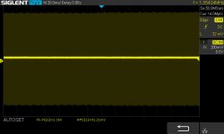
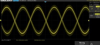
On the Fluke, I now have 41mv of DC output offset (was 36mV before). R8 is too hot after 3 minutes. For the first time, I connected the prototype to the scope and it's worse. See screenshots. The first is without signal and the second with 35mV RMS 1K sine at input.
I'll be good to check everything again. 😭
I will also remove component sockets that I no longer use. They don't have to improve things.
Stef.
EDIT: HI Tim. We created message at the same time.
The prototype is broken again since yesterday after testing R6 connected to GNDPWR.
On the Fluke, I now have 41mv of DC output offset (was 36mV before). R8 is too hot after 3 minutes. For the first time, I connected the prototype to the scope and it's worse. See screenshots. The first is without signal and the second with 35mV RMS 1K sine at input.
I'll be good to check everything again. 😭
I will also remove component sockets that I no longer use. They don't have to improve things.
Stef.
EDIT: HI Tim. We created message at the same time.
Attachments
Hello Stef,
I have had this experience several times now, that the amp no longer works after a test. What is inexplicable to me is that if I desolder the components and solder the same components onto a new board, the amp works again. I have tried this on purpose, without a realisation of what is actually causing the interference - i.e. the defect - wich part.
Maybe it would help to test what happens if you leave the currentless board on such an electrically conductive foam, so that all capacitors are discharged.
Regards Tim
Last edited:
Tim and Stef,
It is a mind blowing for me how you both self create so many issues. Just follow my schematic and the amplifier will work flawlessly with one and two pairs.
Testing variations is another sorry.
Last week I have finished 5th Q17 and I had no oscillations, no smoke, not even a sigle faulty mosfet.
Now to answer to Tim, BF256A can be used. Toshiba jfet's have better noise, linearity, transconductance etc., but here BF256A can work.
Stef, I do not undestand how a gate resistor get hot. Maybe Q8 & Q10 and Q11 are faulty ?
Regards,
Tibi
PS. Please test what you may have done wrong before posting. This thread is almost a full time job for me. 🙂
Tibi,
I am very grateful to you for this thread, as I have learned a lot with the Q17 experiments and it is simply worth experimenting with them. Of course there are also mistakes, but otherwise we stayed stupid....
Regards Tim
I am very grateful to you for this thread, as I have learned a lot with the Q17 experiments and it is simply worth experimenting with them. Of course there are also mistakes, but otherwise we stayed stupid....
Regards Tim
Hello,
I am trying to visualize the different experiences from the successful and failed experiments through the LTSpice simulation.
In the process, I have come to the following conclusion: The original circuit of the Q17 works in a working range that reacts nearly balanced when excited with square pulses. If parameters are changed slightly, this can very quickly produce needle pulses at the output - which I evaluate as potential oscillation possibilities.
I had reduced R13 to 9.x ohms on an amplifier, at this value the simulation also produces violent needle pulses at very low input signal (5mV peak). If I reduce R13 to 7.5 ohms, then I am in a different working range of the power amplifier and the needle pulses have disappeared in the simulation result. Comparing this simulation to one with Q12 as the MosFET, the behavior of R13=7.5 ohms for the original corresponds to Tibi's suggested R13=27 ohms for the Q12 Mosfet.
I have been aware for some time that the amplifier is very asymmetrical and is also an asymmetrical load on the transformer, but I did not realize until now that R10 and R13 have quite different functions. Therefore, in the schematic attached below, I have chosen R10 to be significantly larger than R13 (I am using the designation from Tibi's original schematic here so that you can allocate the components. In the simulation the names of the components change regularly).
In the simulation I added a resistor before the source of Q6. This has very little influence on the behavior of the amplifier.
With this circuit described here I can simulate small square pulses without needle pulses in the output even with several output pairs at power Mosfet. However, since this amplifier works especially towards high frequencies (the attenuation in the MHz range is lower than with a pair of output transistors), I also used L2 = 20 uH (as Tibi did in one of his last simulations). This inductance effectively reduces the high frequency component so that it becomes comparable to the original circuit.
For me this result from many simulations is a basis to get the deficits of the 3-fold Q17 under control. It is clearly more suitable than the variant with the additional capacitors, which is more of a symptom treatment than a systematic optimization or adaptation of the circuit.
The primary advantage of using a Mosfet as Q12 for me is that I can select R10 with 66 ohms (< 100 ohm) relatively high. This has the advantage that the feedback over the + rail is somewhat damped (that is my objective here).
Regards Tim
Attachments

Hello Tim,
For L2 = 20 uH.
20uH doesn't seem to be a common value. There are many choices in 22uH on Mouser.
P2 proto does not work. I reassembled a complete one (2 pairs) with a new PCB, fresh resistors and checked all the components coming from the first proto. -45v on ignition. No chance. I must have made a mistake somewhere on the PCB or elsewhere. I will let it rest.
Good Luke with the simulations.
Regards,
Stef.
L2 = 20 uH is an approximate value.
There exists a ceramic inductor: FASTRON 1812AS 15 µH which is a bit smaller, has a relatively high internal resistance of 10 ohms, so you should reduce R6 and is rated for 170mA. I would expect that to work just okay.
There exists a ceramic inductor: FASTRON 1812AS 15 µH which is a bit smaller, has a relatively high internal resistance of 10 ohms, so you should reduce R6 and is rated for 170mA. I would expect that to work just okay.
Last edited:
I also put together two versions. One mini version and one with two pairs. The mini version ran, but very unstable, the 1kHz square is very bad, the 20kHz square looks like a saw. Two times the output transistors burned out for no reason. With two pairs it didn't even start. I will try to make a new board and move the coil away .No chance.
Stef.
Many boards were made at the beginning of the thread, but no results are seen here. Also would like to see 1kHz and 20kHz quadrature. The amplifier is very unstable.


- Home
- Amplifiers
- Solid State
- Q17 - an audiophile approach to perfect sound