In current configuration, FQP's sound considerably better than anything I have tested, including bipolars.
If anyone know a better pair, I'll be happy to test.
Regards,
Tibi
If anyone know a better pair, I'll be happy to test.
Regards,
Tibi
Hello again,
I have a weird problem for you.
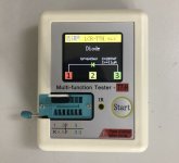
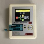
The FQP3P20 do not pass on the tester. I tried all the different MOSFET models that I have in stock, only the FQP3P20 does not pass. Almost all of them display a "diode". One only pass.
I have an old blue T7 tester. They do the same thing (but 3 FQP3P20 pass the test).
I manually tested the dozen FQP3P20 that I have with a small homemade circuit. They all works.
Does anyone have an idea of the cause of the problem?
I really have a knack for running into weird problems.
Regards,
Stef.
I have a weird problem for you.
The FQP3P20 do not pass on the tester. I tried all the different MOSFET models that I have in stock, only the FQP3P20 does not pass. Almost all of them display a "diode". One only pass.
I have an old blue T7 tester. They do the same thing (but 3 FQP3P20 pass the test).
I manually tested the dozen FQP3P20 that I have with a small homemade circuit. They all works.
Does anyone have an idea of the cause of the problem?
I really have a knack for running into weird problems.
Regards,
Stef.
Attachments

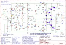
Here is my simulation with mosfet CCS. Notation is different.
Indeed R10 and R13 must be lower. In ~ 27ohm - 30ohm range.
Simulation is OK.
Regards,
Tibi
Hello Tibi,
What is the advantage to use a MOSFET at this location?
I'm interested because I'm modifying the Mini PCB to try to reduce the output offset, add gate stoppers resistors for Q1 and Q4. I need space. I sacrifice the BD139 on the Mini for this. The ZVN4206AV is a bit smaller than the KSC1845. That would suit me fine.
Regards,
Stef.
- Ersetzen Sie Q12 durch einen n-Kanal-Mosfet. Dazu müssen R10 und R13 auf ~50 Ohm - 60 Ohm erhöht werden, daher nimmt die Verstärkung der Cass A-Stufe ab, wird aber linearer. Der Strom-Dumping-Betrieb wird etwas beeinträchtigt, da die Class-A-Stufe eine möglichst hohe Verstärkung erfordert. Hier ist eine leichte Waage, die ich noch nicht getestet habe. Sie können es versuchen.
Grüße,
Tibi
Hello Stef,
Tibi wrote the above, as a conceivable option for improvement.
If you want to change something in the DC offset, it is necessary to make changes in the ground system of the amplifier. Since Tibi's version with R32 works quite ideally, it is rather a sisyphean task to make any serious improvements here.
Regards Tim
Hi Tim,
I'm working on this story of ground and offset.
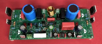
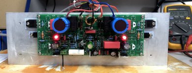
On the new Mini PCB, I moved Q7 and associated resistors to a better location. I added gate stopper resistors for Q1 and Q4. R6 and R32 are now side by side and close to the GNDPWR. Currently, R6 is still connected to GND but it will be easy to move R6 to GNDPWR if needed. I also modified many tracks and reduced the use of VIAS from 8 to one. Q12 is now a ZVN4206AV.
I'm going to experiment with a P2 prototype board that I built with a single pair of FQAs. Several components are socket mounted to facilitate testing. I just finished building the board but haven't tried it yet.
Regards,
Stef.
I'm working on this story of ground and offset.
On the new Mini PCB, I moved Q7 and associated resistors to a better location. I added gate stopper resistors for Q1 and Q4. R6 and R32 are now side by side and close to the GNDPWR. Currently, R6 is still connected to GND but it will be easy to move R6 to GNDPWR if needed. I also modified many tracks and reduced the use of VIAS from 8 to one. Q12 is now a ZVN4206AV.
I'm going to experiment with a P2 prototype board that I built with a single pair of FQAs. Several components are socket mounted to facilitate testing. I just finished building the board but haven't tried it yet.
Regards,
Stef.
Attachments

Last edited:
Hello Tim,
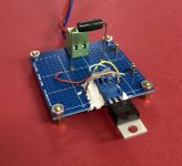
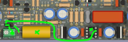
For the moment, the new prototype is burning (a resistor somewhere but I didn't have time to see) and the FQPs become very hot when I connect the two FQA. I had time to read 2.6v of offset at the output.
Without the FQAs, nothing burns. I was able to measure quietly. The measurements appear to be around the simulation values.
The attached measure picture are without FQAs Q15 and Q16.
I look for...
Steve.
Attachments
Hello Steff and Tim,Hello Stef,
Tibi wrote the above, as a conceivable option for improvement.
If you want to change something in the DC offset, it is necessary to make changes in the ground system of the amplifier. Since Tibi's version with R32 works quite ideally, it is rather a sisyphean task to make any serious improvements here.
Regards Tim
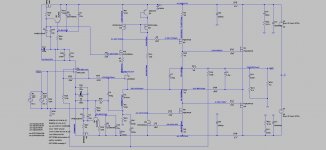
Q12 together with Q6 will form a CCS that bias class A stage. The stability of this CCS is mainly given by Q12, so at a first glance, a bipolar transistor will make sense here. Using a mosfet is just an exercise to hear a different approach. I expect that this "bad ccs" to perform sonically better.
Also Vbe and Vgs versus temperature have different variation transfer functions, mosfet CCS may match better Q17 power stage that is mosfet as well.
What else you may try ?
Change Q7 for JFET. 2SK117GR may be an option and maybe 2SK30GR.
Regards,
Tibi
Hi Tibi,
Thanks for the explanation. I'll try to do most of the test I can do.
Can you remind me of the transistor types good for Q12?
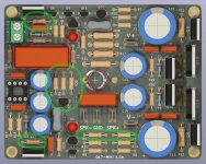
At the moment, I'm still struggling to find the problem on the new prototype. I've finished to measure (still without Q15 and Q16). See picture.
I have R3 and R8 that get hot after a minute or two. Then I cut.
The prototype uses the same components as the Mini except for Q9 and Q10 (BS250P in the built Mini, ZVP2106A in the prototype). I no longer have BS250P in stock.
I also no longer have an op-amp like OPA1641 or OPA 1611 so I put an OPA627 in the meantime.
The current power supply is a little strong (58v) but I have nothing else available and I no longer touch my Q17-Mini which works very well and serves as a reference.
Regards,
Stef.
Thanks for the explanation. I'll try to do most of the test I can do.
Can you remind me of the transistor types good for Q12?
At the moment, I'm still struggling to find the problem on the new prototype. I've finished to measure (still without Q15 and Q16). See picture.
I have R3 and R8 that get hot after a minute or two. Then I cut.
The prototype uses the same components as the Mini except for Q9 and Q10 (BS250P in the built Mini, ZVP2106A in the prototype). I no longer have BS250P in stock.
I also no longer have an op-amp like OPA1641 or OPA 1611 so I put an OPA627 in the meantime.
The current power supply is a little strong (58v) but I have nothing else available and I no longer touch my Q17-Mini which works very well and serves as a reference.
Regards,
Stef.
Attachments
Stef,
The best way to test the amplifier is by NOT eliminating sections.
In this case without output transistors you do not have negative reaction and one transistor in class A stage will get saturated
Q17 was designed to work as whole.
Make sure your PCB is correct and with all components mounted test the amplifier. You may use test points I provided to you.
For Q12 you may use almost any mosfet. 2N7000 may be a candidate. Use thermal glue to have this in contact with heatsink.
Regards,
Tibi
Tibi,
In the Mini, I use BD139 for Q12 and ZVN4206AV for Q8. Same on the prototype.
With Q15 and Q16 when I switch on the PSU, I got 300W on the main wattmeter and the fuse on negative rail (1A) burnt after 2 secondes.
I will check the transistors.
Stef.
In the Mini, I use BD139 for Q12 and ZVN4206AV for Q8. Same on the prototype.
With Q15 and Q16 when I switch on the PSU, I got 300W on the main wattmeter and the fuse on negative rail (1A) burnt after 2 secondes.
I will check the transistors.
Stef.
Hello,
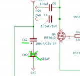
I found the problem with the new prototype. It works now.
I made the dumbest mistake of the year. I wired the strap of the second footprint of C2 with enamelled wire...
It consumes 16W and 37mV offset at output. I haven't measured yet. Maybe tonight.
I will be able to start various tests now.
Regards,
Steve.
Attachments
R8 is connected to the gate of a MOSFET, there should be virtually no current going through it. Do you have a short on the PCB or MOSFET pins? Have you checked to see if the amp is oscillating?
Hello,
I just did a mistake. The board was not working as C2 was not connected to ground. The jumper was made by mistake with a no conductive enamelled wire. The card has been on for a while in the photo position. Almost nothing gets hot.
I haven't taken any measurements yet. Maybe this evening.
Stef.
I just did a mistake. The board was not working as C2 was not connected to ground. The jumper was made by mistake with a no conductive enamelled wire. The card has been on for a while in the photo position. Almost nothing gets hot.
I haven't taken any measurements yet. Maybe this evening.
Stef.
Attachments
Hello,
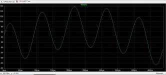
I have added a JFET to the simulation and found that the OPA has a very small DC offset. This has spurred me to modify the circuit so that I can realize a circuit with probably small DC offset without DC servo - i.e. without capacitor in the signal path, in our case the C7.
The high frequency errors are also exemplary low with this circuit and I adjusted the other filters incl. the current damping bridge to achieve ideal results.
I think, this can become a very inexpensive amplifier, without particularly exotic components.
Grüße Tim
Addition:
The 1st frequency response is for an impedance of 12 ohms, i.e. when the loudspeaker has a higher impedance in the high frequency range,
the 2nd FR - last picture - is at 4 Ohm load.
Attachments


Last edited:
Stef, so the feedback was open circuit, that would surely cause bad oscillation.Hello,
I just did a mistake. The board was not working as C2 was not connected to ground. The jumper was made by mistake with a no conductive enamelled wire. The card has been on for a while in the photo position. Almost nothing gets hot.
I haven't taken any measurements yet. Maybe this evening.
Stef.
300W on the main wattmeter and a dozen 1A fuse the joke. !!
😉
I just discovered a funny behavior.
If I press more or less hard with my finger on the big white capacitor (bypassed) at the input or on the op-amp, the output offset changes. By pressing the right pressure, I even manage to set the offset to zero. If I do the same thing with a screwdriver, nothing changes.
This is not a joke.
Have a good evening,
Stef.
Stef, one of the polarities are connected to the shell of the capacitor usually, you are changing the capacitance of the cap.300W on the main wattmeter and a dozen 1A fuse the joke. !!
😉
I just discovered a funny behavior.
If I press more or less hard with my finger on the big white capacitor (bypassed) at the input or on the op-amp, the output offset changes. By pressing the right pressure, I even manage to set the offset to zero. If I do the same thing with a screwdriver, nothing changes.
This is not a joke.
Have a good evening,
Stef.
I have this circuit at input.
Only the 1uF white cap (CDE) and the opamp do that. NO the PCB, the transistors or the big chemical caps.
Seems related to the opamp input.
And only with my finger. Tibi invented the amp that is controlled by finger and ear. 😉
I measured the voltages. I don't know if R3 and R13 are ok. The measurement at R15 seems to be very out of step with R14.
Regards,
Stef.
Attachments

- Home
- Amplifiers
- Solid State
- Q17 - an audiophile approach to perfect sound