Highly suspicious. From your pic the second from left looks fake as well.Yeah, give 'em a go. You'll need at least 36 to build the Q-grossDAC.
The variations of labelling I've seen are these 4.
Logo is subject to the copyright laws. There are two ways to avoid litigations. Make a logo to look inrecognizable or remove logo completely.
EDIT: Font is different. Font design is also subject to copyright laws.
Last edited:
You look from a designer point of view. Yes, it can be better. Always we can make it better... However I don't want to distract you from releasing a final project, I want my kit shipped now 🙂🙂🙂🙂🙂 , now 🙂🙂🙂🙂🙂, now 🙂🙂🙂🙂🙂 and what I do propose doesn't change a design.I've pondered this idea @sajunky and I can't think of any advantage of spreading out the 36 DAC chips over two boards rather than one. Perhaps if they were running above 5V and getting warm this would allow them to run cooler by spacing them apart. Or perhaps if you wanted to get the maximum sample rate out of them you could do this as the HC86 which drives them doesn't have very high drive ability when running at 2.5V as in this design. But a better solution might be to raise its supply voltage (change the LED which is a shunt reg to a higher voltage one) so as to improve its drive ability. Going much above 3.3V (not sure which LED would give this mind, perhaps remove the shunt LED and run direct from the DAC supply) you'd want to swap HC86 for HCT86 to preserve logic level compatibility on the I2S inputs.
You're right, the extra cost of two PCBs is going to be relatively small, given how cheap PCBs are these days.
Yes, you seem have overlooked the fact that there is lot of 192kHz source for download. Also the optimal conversion rate from SADC (DSD64) and DSD128 source is 176.4kHz. TDA 1387 chip can handle much more. We discussed it already and I was satisfied from your report that with the current filter setting sample rate 88.4kHz brings minimal deviation to the frequency plot, the same probably with 96kHz. If someone wants to go 176.4/196kHz, (I want to try), then spreading out 36 DAC chips over two boards would help clocking these chips properly with reduced jitter. Some others would like to use bypasing film capacitors, there is more space to do so.
It was a discussion running already. This time I wanted to show that spreading out chips has practical advantage. It is easier to find a fault. Owners of H-DAC version would perhaps want to keep a fifth board as a spare. Replacing a faulty board is quicker than finding a fault on the board.
You look from a designer point of view.
Well yeah, duh 😀
Yes, it can be better. Always we can make it better... However I don't want to distract you from releasing a final project, I want my kit shipped now 🙂🙂🙂🙂🙂 , now 🙂🙂🙂🙂🙂, now 🙂🙂🙂🙂🙂 and what I do propose doesn't change a design.
So long as your kit is the most basic level one (nothing pre-assembled at all) then yeah, this doesn't change the design.
Yes, you seem have overlooked the fact that there is lot of 192kHz source for download.
Wouldn't that all be 192k/24 rather than 192k/16 though?
Also the optimal conversion rate from SADC (DSD64) and DSD128 source is 176.4kHz.
First I've heard of that - got any links I can follow to learn up on why this would be so?
TDA 1387 chip can handle much more. We discussed it already and I was satisfied from your report that with the current filter setting sample rate 88.4kHz brings minimal deviation to the frequency plot, the same probably with 96kHz.
Maybe a boost in the FR of 1 to 2dB at the top end.
If someone wants to go 176.4/196kHz, (I want to try), then spreading out 36 DAC chips over two boards would help clocking these chips properly with reduced jitter.
Yep, but then why stop at removing half the chips? Taking 75% of them off will reduce jitter even more 😀 (only half serious).
It was a discussion running already. This time I wanted to show that spreading out chips has practical advantage. It is easier to find a fault. Owners of H-DAC version would perhaps want to keep a fifth board as a spare. Replacing a faulty board is quicker than finding a fault on the board.
I'm not sure I follow that its easier to find a fault. But maybe it is as even with 36 chips you can start by isolating which board - which is the first stage of a binary search. But then you're down to individual chips.
Btw - if you really really don't want to distract me, keep what you actually plan to do off the thread, at least until kits are available 🙂
Oh and regarding fake chips, there are 5 different variants of the one you reckon is a fake on my desktop. That's not proof of course but renders it less likely its a faked one.
Last edited:
That is a main point, just a BOM for an extra PCB.So long as your kit is the most basic level one (nothing pre-assembled at all) then yeah, this doesn't change the design.
It depends on the NV data content of USB bridge. Device driver will expose device capabilities to the user. The best if it matches capabilities of our DAC chip. Generic USB bridges will expose maximum capabilities of the USB chip instead, but we can select sample rate and bit depth either on the DS control panel or in the app when working in WASAPI exclusive mode. Everything above 16-bit is accepted as 16-bit (ignoring number of LSB's), but a clock rate is increasing wasting bandwith.Wouldn't that all be 192k/24 rather than 192k/16 though?
I can find links saying that DSD quality is comparable with 24/88.2kHz PCM, some say it is higher, but nobody wants convert DSD content to 44.1kHz with a lot of ultrasonic content, it is for sure. For the purpose of this thread I will end on this assessment.First I've heard of that - got any links I can follow to learn up on why this would be so?
It was noted already and fully accepted.Maybe a boost in the FR of 1 to 2dB at the top end.
Simple calculation for a clock load. If a given clock works fine with 36 chips @96kHz, then reducing load capacitance in half is expected to work @ a double rate. It is not enough, as higher sampling rate requires a lower jitter. I could further demand for 1/4 (9 chips), but I want to try 18 chips first. 🙂Yep, but then why stop at removing half the chips? Taking 75% of them off will reduce jitter even more 😀 (only half serious).
.LOL. Of course I will bring sensitive matters in private and I promise, it will never come out.I'm not sure I follow that its easier to find a fault. But maybe it is as even with 36 chips you can start by isolating which board - which is the first stage of a binary search. But then you're down to individual chips.
Btw - if you really really don't want to distract me, keep what you actually plan to do off the thread, at least until kits are available 🙂
No progress on this particular DAC as we're rather in suspended animation here in China at present as regards business. I needed to get some transformers made at a factory nearby but they've not returned to work yet after the CNY holidays due to nCoV (or whatever its new name is). I've been focussing my efforts on revising the design of the PhiDAC (on the lingDAC thread).
hopefully things will get better soon. I have a couple of ordered placed in January that has no movements but has since been shipped out this past week. there must have been a huge backlog.
A nice packet of 100 dac chips turned up today, so I guess some of the backlog is clearing a bit.
Our local transformer factory has been back at work for a few days now but they've told us they've such a backlog that it'll be the end of March at the earliest when they can get around to serving us. I've just about firmed up the design for the next generation PhiDAC now though so will be focussing on that for the next couple of weeks, along with the CPU project.
Thanks! Keeping the creative juices going seems to be essential to my sanity so please don't look on these designs as altruism 🙂
Of course! It's good to keep the Grey Matter active - use it or lose it!
Just wondering where I can read about this one..
along with the CPU project
Just wondering where I can read about this one..
I don't wanna be 'that guy' and keep asking if this one is still in the works..
But I still really like the look of this project and gonna be 'that guy'..... 🙂
But I still really like the look of this project and gonna be 'that guy'..... 🙂
I've put this one into suspended animation as I'm getting equivalent or even slightly better results with my PhiDAC hex for a lot less effort in the build.
You're keen to go ahead with a build of this? If so what would you like from me to assist with that?
You're keen to go ahead with a build of this? If so what would you like from me to assist with that?
I'd be interested in the (rather daunting) challenge of putting together a Half-Gross.
I've got as far as buying 100x TDA1387.
Do you have a working layout already? (silly question as I've seen the pics!). I guess at the minimum, I'd need gerbers (is post 23 the latest?) or happy to purchase prototype boards that you might have spare.
The area I am most unfamiliar with is the transformers.. Do they have to be custom made or can they be bought? Is there a seperate filter board for this one?
And presumably I need an interface such as USB - I2S?
I'll look into what boards I have currently - I'm fairly sure I have plenty as I've only prototyped two and sent one early prototype to an interested party.
The transformers are definitely custom ones. You can buy cores relatively easily (I think at the very least Mouser stocks them but I'd need to check) or if you'd like me to send PCBs I can also send cores. There is a separate plugin board but its a buffer with SMT transistors on it, not a filter. I have several, no trouble to send you one of those already built. The filter's part of the main board - that can be made with either P14 cores (which I have stocks of) or inductors from Mouser. The PCB has been made to accept either.
Yes you will need some kind of interface which spits out I2S.
I'm happy to try and wind my own transformers and P14 cores if you'd be able to supply the cores, PCBs, assembled buffer etc. It'll be an interesting challenge!
Would you be so kind as to PM me with what you can provide with costs, as well as your current recommendation for an I2S converter (I've seen some older posts with a few links)?
Would you be so kind as to PM me with what you can provide with costs, as well as your current recommendation for an I2S converter (I've seen some older posts with a few links)?
Update
We've created an r1 PCB now which incorporates quite a few changes.
First the PCB is now mono, so two are needed to build a stereo DAC. Space ran out incorporating all the mods. EP17 trafos have been ditched in exchange for EE35s which are much bulkier. But it means lower distortion in the LF region which was a major weakness of the first prototype.
Second the filter is now a pluggable item so can be 3rd/5th/7th or 9th order, using the same PCBs as for PhiDAC hex. The component values need to change so PhiDAC filters can't be used directly (the working impedances are different) but at least we won't need to create any new PCBs for GrossDAC filters.
Lastly with two PCBs there are going to be four power supplies available so a full gross DAC can be built, using four DAC PCBs.
Attachments
Hi Richard,
Finally getting the time to look at this build again and I've some questions regarding the transformers if you don't mind.
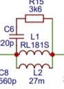
The inductors L1-L8 are shown as pairs on the schematic:
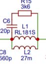
Do I need 2 windings in parallel on the P14 cores, or just a single winding? And am I correct that the target inductance is 27mH total between the pins?
Is the mentioned 6+6t : ~4000t generally right for the EP17 input transformers on a halfGross? This would be CT primary and CT secondary.
And I have the output RM10s as single primary, CT secondary 1:2?
Does any of this look right? This will be my first winding task above 14 turns 😱
Finally getting the time to look at this build again and I've some questions regarding the transformers if you don't mind.
The inductors L1-L8 are shown as pairs on the schematic:
Do I need 2 windings in parallel on the P14 cores, or just a single winding? And am I correct that the target inductance is 27mH total between the pins?
I came up with a way to get fewer turns on the transformer - add the CT later with thinner wire. Here I have 6+6 T for the primary (0.62mm) and there's enough room left for 4000T of wire for the secondary (0.05mm). This gives an impedance ratio of ~111k meaning an 11k I/V resistor on the secondary represents 0.1ohm to the DAC array. Initial listening indicates a slight improvement in LF - the price is the need for a lot more DAC chips - at least 128.
Is the mentioned 6+6t : ~4000t generally right for the EP17 input transformers on a halfGross? This would be CT primary and CT secondary.
And I have the output RM10s as single primary, CT secondary 1:2?
Does any of this look right? This will be my first winding task above 14 turns 😱
Attachments
- Home
- Source & Line
- Digital Line Level
- Grossly parallel multibit DAC adventures