That's a lot of amplifiers Sajti.
Yes, but I did mistake with 2SC2240/2SA970, when I ordered only 100-100pcs, before Toshiba finished manufacturing them...
So my current amplifier use 12-12pcs of 1845/992 for one stereo pair.
Sajti
Yes, but I did mistake with 2SC2240/2SA970, when I ordered only 100-100pcs, before Toshiba finished manufacturing them...
So my current amplifier use 12-12pcs of 1845/992 for one stereo pair.
Sajti
The 2SC2240/2SA970 are very nice transistors but so are the 1845/992's so all good Satji. My first amplifiers (a long time ago) used cascode input stages using BC550/560's but i much prefer the single transistor LTP input.
Cheers
Q
Just a genuine question - why is everyone so afraid of triple darlington output stages ? It's something I rarely ever see... yet after simulating Leach's low TIM amplifier, they seem really good to me.
Hi jaycee, nothing I suppose except that Darlington configurations aren't as fast or as linear esp. in triples. Modern output transistors have pretty good gain and linearity, I'm using an "output transistor" as the driver in this amp.
But you know my other amp series The "NBIP300" used 2N3773 or MJ15003's and by all accounts they sounded pretty good.
Cheers
Q
But you know my other amp series The "NBIP300" used 2N3773 or MJ15003's and by all accounts they sounded pretty good.
Cheers
Q
well.. with the way Leach has the predriver and driver arrange, they never actually switch off.. which would seem to be a massive advantage to me in terms of linearity. I wont pretend to know the math though 🙂
Some people have said they are difficult to stabilise but I've never had that problem...
Some people have said they are difficult to stabilise but I've never had that problem...
The 2SC2240/2SA970 are very nice transistors but so are the 1845/992's so all good Satji. My first amplifiers (a long time ago) used cascode input stages using BC550/560's but i much prefer the single transistor LTP input.
Cheers
Q
1845/992 are nice, and the most important, that they are still available. Cascode is good solution, I use it in some location, mainly in VAS.
Sajti
Just a genuine question - why is everyone so afraid of triple darlington output stages ? It's something I rarely ever see... yet after simulating Leach's low TIM amplifier, they seem really good to me.
I use only triple darlingtons, they have many advantages comparing to the double.
Sajti
It is a buffered single vas, topsy turvy drawn. And a little modulation of the current source by that buffer... helps a tiny bit with the amplification....this in the schematic* of my old Yamaha Rx-777 receiver...
For these kind of stages (with bias networks and single-double-triple output stages) I would choose a Sziklai with cascode configuration. It is the most important gain stage of the amplifier and much comes into play here: minimum load on the first stage (ok), high gain (ok), low cob effect - high frequency roll off (ok), temperature stability (ok). Hardly seen anywhere, demands some more design muscle and resources.
Maximum output swing ('rail to rail' and thus maximum output power) seems to be important for many, but that is rediculous if optimum performance is traded in for it.
If this stage is performing well, the output stage has only two important specs to meet, having a flat beta of a broad range and being capable of carrying sufficient current into the load. That's a challance on its own, and maximum output voltage swing is without these useless. If the output does not follow the input (through the feedback network to the input differential) anymore because of current deprivation, the amplifier gain stages will be 'stressed' in corresponding amounts of their open loop gains, causing unlinearities, errors and other nasty havoc. And that poor second stage has to feed the increasing hungry end stage more and more (base current in bjt's, or, comparable, charge-discharge current in mos), until collapse.
Stinginess as a design guide, why not.
I had to comp the VAS stage way more heavily with darlingtons over MOSFETS. A triple config with just slow it down more. It is the turn off current you have to worry about with transistors.
If you were to use a triple stage with 100 ohm on the first pair, 20 ohm on the second and .22 on the outputs, speed should be good. the VAS loading will be very close to a darlington config.
I am going to try a MOSFET - BJT config when I have some time.
If you were to use a triple stage with 100 ohm on the first pair, 20 ohm on the second and .22 on the outputs, speed should be good. the VAS loading will be very close to a darlington config.
I am going to try a MOSFET - BJT config when I have some time.
Interesting idea of using a triple EF output stage.
Using C5200/A1943, beta is flat to 80 up to Ic of 7A. This is an Ib of 87.5mA at a 7A speaker load.
Choosing Drivers could be TT400A/C (replacements of the C4793/A1837) with 100MHz, 1.5A and 160V the beta is flat to 200mA and is around 150. This means the Ib is only 580uA, and even if you set the driving VAS at 6mA this would give us the bridge ratio, 10:1.
I see no requirement for a triple EF OPS until we get to 2-3mA Ib for the drivers. This is mandated only with a 350W plus amplifier using older, less modern output devices. These figures are taken from the curves of the datasheets.
HD
Last edited:
Member
Joined 2009
Paid Member
Just a genuine question - why is everyone so afraid of triple darlington output stages ? It's something I rarely ever see... yet after simulating Leach's low TIM amplifier, they seem really good to me.
more likely to oscillate perhaps
why is everyone so afraid of triple darlington output stages ?
Good question. Worth the time.
1. First of - the lack of practical examples how to stabilize it over the wide range of reactive loads. EF triple without special care are unstable. You assemble the amp, set modes and bias currents, let it preheat. Then you feed the signal and OPS are naturally burning PCB traces or trannies.
2. Second of - the lack of "easy-to-understand" guides what to do and how stabilize it. Most of designers of popular amp's designs can say only 'l've test it and it works'. No time is spended to carefully explain why this is made so. This is something like payed knowledge and profitable business.
3. Third of - EF triple like a drug. It's hard to stop when you try. And you will ask for more and more until unstable region will be achieved. And, of course, you'll feel the power of First and Second. Have no doubt.
There are two practical ways to build stable EF-triple.
1. Build relatively slow and, let me say narrowband, EF triple. You need to slowdown second stage. This is easy, just put ~100-150 ohm at driver's base and ~100-150 pF base-collector. This approach must be named "off first stage at HF MHz range". Doing so you literally convert EF3 to EF2 which is much more stable.
2. Build relatively fast, and let me say racing car, EF triple. You need to exclude ten MHz behavior of last stage by using relatively slow trannies like MJL21193/4 simultaneously with providing huge-SOA driver stage which will feed the load through Cbe of the last stage. Say 3 pair of KSC2690A/A1220A. This approach must be named "feedthrough last". Doing so will again convert EF3 to EF2, but different way.
Think about EF stage as impedance converter, derivative function vs freq. EF1 converts resistive source impedance to inductive output impedance. EF2 converts resistive to inductive^2 which is inherently unstable with even ten-pf load, so for obtaining stability you need to place ten-pf capacitance at the EF2 input (for converting source impedance to capacitive and having inductive^1 at the output) or decouple any load capacitance with nearly placed inductor.
There we see ten-pf capacitance which is ideal for VAS load point, so we could go ahead and further put EF3 with decouple inductance. This will mostly do the job, but we will anyway want more and more feedback depth. Have no doubt, we will reach instability while trying to close the loop through output inductor and we need to split feedback path to "before inductor" after ones of MHz and "after inductor" through audioband to exclude inductor parasitic resistance influence to damping factor.
Next item for accounting is huge fT vs current deoendance for relatively high fT power trannies. Just compare MJL21194 graph with MJL3281. This is load-outputcurrent depended frequency pole. And being designer you need to close feedback loop independant of this, read as 'strictly before' those freq's. Or pay special attention to compensate those effects.
Thanks for the input guys.
MarsBravo; Yes the Yamaha schematic is "topsy turvy" with neg rail at the top. It is a snip from the full schematic where the other channel is drawn "right way up". But that shows the signal path in bold lines making it less clear. I had to turn my head a couple of times too 🙂. My desire to go rail to rail has a little bit to do with efficiency, but the main reason for my split rail design is I do not want the input, VAS and driver stages running out of voltage during high power output and clipping. I want a little left even when the output stage clips. Note; the 85v rails will be regulator fed so there is no droop during high power output.
AKSA; As you suggested I'm relying on the gain of better power transistors to do the job. The NJW0281 & NJW0302 have a minimum gain of around 75 at 4 amps (typ 100) which is why I'm also using them as the driver. They are linear too to 4 amps and have a fT of 30 Mhz. Pretty good me thinks.
BesPav: Great insight & detail. Thanks for taking the time time to think it through and express it. I learnt a bit about stability and driving capacitive loads in my NMOS quasi-complementary series. Some constructors had stability problems because they didn't pay enough attention to quality components, good grounding and other routing techniques. A tiny thing like grounding the VAS heatsink made a bigger than expected improvement. Other constructors, with some good notable exceptions, re-designed the PCB with disastrous results - go figure.
Thanks to the other members as well, your comments and recommendations are well noted.
I'm close to the final schematic and the PCB is almost complete. I'll post it here first and then maybe start a new thread around the amp project itself.
Cheers
Q
Great insight & detail
Do forum needs dedicated thread about?
NMOS quasi-complementary series
Creek4330-like with differential drive of the OPS's LTP.
Very high bandwidth, very high intrinsic feedback depth and very short path around OPS.
Also check Kendall Castor-Perry article about class-i.
The NJW0281 & NJW0302 have a minimum gain of around 75 at 4 amps (typ 100) which is why I'm also using them as the driver. They are linear too to 4 amps and have a fT of 30 Mhz.
Pay special attention for keeping inside SOA and huge fT/Ic drop being overloaded. Unpredictable woofer circumstances and mass-reactive behavior could demand up to 3x SOA vs resistive load and up to 2x current being hard-drived.
Hi folks,
I'm working on another amp and have some decisions to make around the second stage. I could go the MJE340/350 (stand alone or darlington/ compound / cascode) but I like the idea of faster & more linear devices. Finding one that will take a bit of heat is difficult, hence my question; Is it ok to parallel them. In this example it is T9-T12 and I'm thinking 2 each of 2SA1381 & 2SC3503.
Naturally I will match them so I feel it's ok, but have I missed something?
Cheers
Q
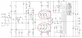
check out schematic Linn Klout, first PDF in post #52 under
tweaking classic Linn LK1 & LK2 / LK280
Thanks tiefbassuebertr!
I presume you are talking about this arrangement*. Yes this is what I was thinking as well, although in a different stage configuration. Thanks for the find.
* Source: LINN, Service Manual for LK2 Series of Power Amps. Copyright 2000 Linn Products Limited.
Cheers
Q
I presume you are talking about this arrangement*. Yes this is what I was thinking as well, although in a different stage configuration. Thanks for the find.
* Source: LINN, Service Manual for LK2 Series of Power Amps. Copyright 2000 Linn Products Limited.
Cheers
Q
Attachments
Curious design with the second stage in a 'half-fixed differential pair of Q9-Q10, doubling the drive through the mirror of Q16-Q17. Q10 is in the very centre of this configuration, compensated with C5 and C6-R12. Must run a fair amount of current to have the Q19-20-21--Q25-26-27 driven properly, which themselves sum their signal current into Q23-24. What is the ultimate reason for three in parallel io one single here?
Q23-24 might be singelton's, can be darlington's.
Power supply suggests only a moderate power amplifier (317-337).
Q23-24 might be singelton's, can be darlington's.
Power supply suggests only a moderate power amplifier (317-337).
Curious design with the second stage in a 'half-fixed differential pair of Q9-Q10, doubling the drive through the mirror of Q16-Q17. Q10 is in the very centre of this configuration, compensated with C5 and C6-R12. Must run a fair amount of current to have the Q19-20-21--Q25-26-27 driven properly, which themselves sum their signal current into Q23-24. What is the ultimate reason for three in parallel io one single here?
Q23-24 might be singelton's, can be darlington's.
Power supply suggests only a moderate power amplifier (317-337).
Might be to share dissipation?
Cheers
Q
Hi Quasi,
Maybe consider the TO220 MJE15030/31 as drivers. They are 4A, 30MHz, and good linearity with high capacity for dissipation, I think up to 25W. They would be a better device than larger TO3P devices unless you are using four pairs of outputs.
HD
Maybe consider the TO220 MJE15030/31 as drivers. They are 4A, 30MHz, and good linearity with high capacity for dissipation, I think up to 25W. They would be a better device than larger TO3P devices unless you are using four pairs of outputs.
HD
- Home
- Amplifiers
- Solid State
- Second Stage. Paralleling transistors ok?