Farnell sells or used to sell 28.224 MHz crystals. In fact I originally intended to use a 28.224 MHz crystal for my valve DAC, with a reactance-valve-tuned valve oscillator phase-locked to the incoming sample rate by a solid-state PLL, until I found out that I couldn't make a large enough tuning range with a reactance valve. I then went for a 27 MHz fixed oscillator and asynchronous sample rate conversion.
For 112.896 MHz, you would probably need a PLL or a specially-made overtone crystal.
For 112.896 MHz, you would probably need a PLL or a specially-made overtone crystal.
And won't such fast shifting of a logic also introduce distortion phenomena from the logic itself? E.g. due to different rise and fall times?
Anyway ... "a 1.536 MHz R2R DAC would be simple" ... 1.536 MHz conversion clock derived from a super stable 6.144 MHz crystal - which is then again clock multiplied to the frequency needed to feed the I2S data line .. which is less influenced by not-so-perfect phase noise specs. But then again, maybe a perfect R2R DAC isn't that simple to make ....
... thinking aloud here in the morning ...
Cheers,
Jesper
Hi Jesper!
Settling time of that R2R dac would have to be impeccable to actually get decent resolution out of it, at those speeds.
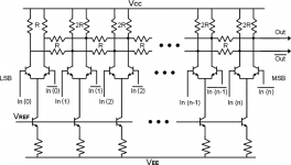
R1 and R4 serve as common resistors for all transistor collectors, so all taps/transistor collectors share the same R1 and R4.
By a (one) tap you mean a balanced pair of npn transistors with their current source, right?
So right now all positive phase transistors (collectors) all share R1, the negative phase (collectors) all share R4, so all collectors of similar phase are connected to eachother.
I can imagine this causing problems.
Thank you for the clarification. I understood what you meant. I agree with you that one resistor for many transistors is one of the reasons for the oscillation. I know 24taps is more unstable than 12taps. But many transistors sharing one resistor is the essential know-how in analog FIR architecture. The attached pic is FFT of 1tap; SN=88.3dB at -32.56dBFS. If you have 36taps, you have 31.1dB gain, which results in -32.56+31.1=-1.46dBFS, while the noise floor is almost the same value as 1tap. So, your SN with 36taps means 88.3+31.1=119.4dB, ideally. It's impossible to have ideal value on the real PCB. What I need to do is to make real PCB ideal as possible as I can. The real value I can have now is almost 117dB. It's not bad but not ideal.
The magic of analog FIR is a simple addition of the gain without an increase in the noise floor. Paralleling two DACs has 6dB gain, but the improvement of SN is 3dB, not 6dB. Analog FIR is the magic that has 6dB improvement in SN by doubling. The point of magic is an accurate phase relation between transistors. The best way to have the accuracy is to share one resistor. I have tried to insert a buffer amp to separate transistors, e.g., 12taps with buffer and 12taps with buffer. But buffering destroy accurate phase relation, which ends up poor SN.
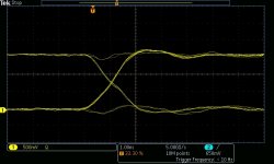
The 2nd pic is the base of the positive transistor and negative transistor. The propagation delay between low to high and high to low usually isn't the same, including rise and fall time. This is precisely an adjusted one because 100ps accuracy is mandatory for more than 110dB SN in my experience. Clock jitter must be as small as possible. As long as I have experienced on the real PCB, gate logic(I/O buffer with FF in FPGA) is more dominating than the clock itself. 30ps is my rough estimation of gate logic jitter. I don't think discrete logic on the real PCB driven by 100MHz clock with many fanouts can have better value than this, though I know it's controversial.
As to RTZ, fast discrete logic has considerable over and undershoot. You can't have a clean waveform like the 2nd pic.RTZ has more toggling than NRZ. If you can have an accurate pulse duration between low and high, The advantage of RTZ disappears. The disadvantage remains; less SN because of less signal amplitude. That's the reason I don't want to employ RTZ. Precise pulse adjustment is better than RTZ, IMHO.
Attachments
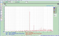
Thank you for the clarification. I understood what you meant. I agree with you that one resistor for many transistors is one of the reasons for the oscillation. I know 24taps is more unstable than 12taps. But many transistors sharing one resistor is the essential know-how in analog FIR architecture. The attached pic is FFT of 1tap; SN=88.3dB at -32.56dBFS. If you have 36taps, you have 31.1dB gain, which results in -32.56+31.1=-1.46dBFS, while the noise floor is almost the same value as 1tap. So, your SN with 36taps means 88.3+31.1=119.4dB, ideally. It's impossible to have ideal value on the real PCB. What I need to do is to make real PCB ideal as possible as I can. The real value I can have now is almost 117dB. It's not bad but not ideal.
The magic of analog FIR is a simple addition of the gain without an increase in the noise floor. Paralleling two DACs has 6dB gain, but the improvement of SN is 3dB, not 6dB. Analog FIR is the magic that has 6dB improvement in SN by doubling. The point of magic is an accurate phase relation between transistors. The best way to have the accuracy is to share one resistor. I have tried to insert a buffer amp to separate transistors, e.g., 12taps with buffer and 12taps with buffer. But buffering destroy accurate phase relation, which ends up poor SN.
The 2nd pic is the base of the positive transistor and negative transistor. The propagation delay between low to high and high to low usually isn't the same, including rise and fall time. This is precisely an adjusted one because 100ps accuracy is mandatory for more than 110dB SN in my experience. Clock jitter must be as small as possible. As long as I have experienced on the real PCB, gate logic(I/O buffer with FF in FPGA) is more dominating than the clock itself. 30ps is my rough estimation of gate logic jitter. I don't think discrete logic on the real PCB driven by 100MHz clock with many fanouts can have better value than this, though I know it's controversial.
As to RTZ, fast discrete logic has considerable over and undershoot. You can't have a clean waveform like the 2nd pic.RTZ has more toggling than NRZ. If you can have an accurate pulse duration between low and high, The advantage of RTZ disappears. The disadvantage remains; less SN because of less signal amplitude. That's the reason I don't want to employ RTZ. Precise pulse adjustment is better than RTZ, IMHO.
Not sure about what can be achieved on the real pcb regarding signal quality. 30 pS is a low figure with fpga, but you'd have to be really precise about impedance controll and trace length to stay in that region on pcb level. It's a great feature that with fpga you can controll timings this precise, it gives room to adjust which gives it an edge over just hoping pcb traces will work out. What steps/resolution can the fpga provide?
FWIW, just using cmos I always think the sq lacks a certain clean signature, as if there's some noise modulating within the signal that is less there using faster logic like cml. Not sure if it's e.g. just a power supply issue or lack of rise and fall time speed/difference in propagation delays, ISI etc, hence still the RTZ thoughts in the back of my head. The faster and cleaner the logic, the less this is a problem, but what is fast enough is often proven not enough when dsd rates go up. I haven't yet tried to demistify this, but hope to get there in the coming months. I'll get back on this when there's news worth sharing.
I've repeated many times, but 5V CMOS AC logic has LOWEST phase noise of all logic families I've tested - lower then ECL, and far lower the LVDS...
Dropbox - Logic Phase Noise.jpg - Simplify your life
Care has to be taken with CMOS logic due to the shared I/O ground...
Aviod the latest CMOS logic that supports level shifting / Hot Pluging - as level shifting is performed by large value resistors on the logic gate input, this series Gate resistance introduces noise - good old AC logic has non of this...
UHS Tiny Logic has this series input resistor, but the small package size and no issues with shared Ground / PSU between Gates (only Single / Dual Gate) allows us to parallel packages in a tiny area... they also have around 700pS edge times... and matched H/L impedance...
We use ECL where speed is required above say 200MHz, but suffer the higher phase noise...
CML sounds like a good idea, but the small single swings and very small input device geometry (for speed) results in higher LF (close in) Phase noise that matters in our Audio applications.
Also, differential matched impedance design / track lengths to achieve good CM rejection for CML is beyond most DIY designers skill set...
With good / careful CMOS design you can push beyond 130dB Dynamic range... and under -120dB THD at FS...
I've repeated many times, but 5V CMOS AC logic has LOWEST phase noise of all logic families I've tested - lower then ECL, and far lower the LVDS...
Dropbox - Logic Phase Noise.jpg - Simplify your life
Care has to be taken with CMOS logic due to the shared I/O ground...
Aviod the latest CMOS logic that supports level shifting / Hot Pluging - as level shifting is performed by large value resistors on the logic gate input, this series Gate resistance introduces noise - good old AC logic has non of this...
UHS Tiny Logic has this series input resistor, but the small package size and no issues with shared Ground / PSU between Gates (only Single / Dual Gate) allows us to parallel packages in a tiny area... they also have around 700pS edge times... and matched H/L impedance...
We use ECL where speed is required above say 200MHz, but suffer the higher phase noise...
CML sounds like a good idea, but the small single swings and very small input device geometry (for speed) results in higher LF (close in) Phase noise that matters in our Audio applications.
Also, differential matched impedance design / track lengths to achieve good CM rejection for CML is beyond most DIY designers skill set...
With good / careful CMOS design you can push beyond 130dB Dynamic range... and under -120dB THD at FS...
I'm afraid you might be right John. And with "afraid" I mean: my current bet on cml might not be the best.
Let me tell you how I came to this 1 bit endeavour.
Having tried all sorts of no-dac dacs (8 years ago I guess, at least: when Foobar had it's pcm to dsd converter as a plugin), first few things that stood out were the obvious good things, but major let downs were isi distortion. Not having tried out all cmos logic families, but had best results with the Potato's. Sonically this was sonically satisfying, but never got outstanding results.
I turned to the kiss principle and decided to just do 1 bit (no fir etc), for sake of finding the secret ingredients for this recepy.
CML was far better: sonically and measurably.
The problem of dynamic range isn't that big: cmos never lend itself to modulation above -6dB, while with cml this could go all the way up to -1dB (for pcm 0dB to dsd conversion), so it's purely modulator restricted. In other words: I see the same distortion rise at -1dB cml vs -6dB cmos. This means an almost effective doubling of the output singal volume of cml, or other way around: cmos is restricted to half the signal of the 3 or 5 volts supply. I know these dB's are debatable, but it's what I found as a pretty solid rule of thumb.
The analog devices HMC723 is expensive but can deliver 1.5 volts peak to peak with perfect symmetry. That's 1.335 volts at -1 dB.
Cmos, at -6 dB delivers 1.65 volts for a 3v3 supply and a 2.5 volts for 5 volts supplies. That's not a deal breaker. Every volt matters but I can hand solder these things, not be concerned at all about rise or fall times (really well defined energy packets!), supply noise everywhere and always have a really good balanced signal.
I agree on the lf-noise. Cmos beats it, probably by a fairly large margin. But it beats cmos at almost every other typical real world implementation. I have to say I wasn't impressed when I tried 1 ONSemi cml, nowhere near the Analog one, so "just cml" won't do it, just like cmos. The good thing is though, because of the balanced signal there's almost no way of interfering the signal but routing takes a lot more care (and I'm not yet convinced I've mastered it;-)
Oke, this isn't meant as a rant about cmos, I started this by stating I am more or less afraid.
Because cml doesn't scale well to many gates. It either is extremely expensive to use e.g. 8 or more taps, and really hard to get it well implemented on a pcb. It also has it's own drain resistor, so less easy to use in a fir topology, though that can be overcome with serial resistors (which I absolutely try to avoid).
Also in that regards, xx3stksm is covering new grounds and scaling it up as well as keeping it economical.
I might be back here in 6 months or so saying "Hey John, thanks for the heads up, you were right all along".
But for now, it's almost always very easy to correlate measurements with sq, pinpoint every characteristic of the board, clock, power supplies etc, which was the reason I went for this. For now at least.
By the way, do you (always) use rtz or similar encoding, or does the UHS family provide enough quality to not having to use it?
I couldn't find any cmos family (hand solderable), to work error free at dsd512, allways went fine up to dsd128, maybe 256 but above none were free of modulation at -40 to -60 dB, be it fir, balanced or whatever, never clean. Hence the cml path..
I'm afraid that the subject RTZ is very miss-understood here on the forum, with a whole load of rubbish spouted I cannot it even get my head around to understand.
Things like needing to insure matched edge times? RTZ is no different to "unmodified" pulse stream in this respect - only that you have more edges with RTZ.
Edge differences are "cancelled" by insuring you always have one rising and one falling edge for each pulse edge - ie. a true differential arrangement.
RTZ function is to insure that the energy contribution of each pulse is independent on the previous or next pulse... The pulse is returned to zero before the next pulse cycle.
Without RTZ you will have increased THD + Noise as there is an inherent system non linearity - which unless you have infinitely fast pulse edges cannot be resolved...
I really dont understand all this rubbish about the need for perfect matched edge speeds with RTZ... its just total nonsense... I dont know who started it, but its creates confusion and misunderstanding and seems to have been accepted as fact!
The ONLY requirement is that each individual pulse - think packet of energy (Positive or Negative) has EXACTLY the same energy contribution over time. With a 1 bit system, you want 120dB Dynamic range then each pulse must impart a "packet of energy" accurate to 1ppm... If the edge speeds are mismatched it does not matter just as long as they have the same missmatch for each and every pulse - positive or negative going...
The important point to note is that the shape of the pulse is not important - just that the energy contribution of each pulse remains identical - you could have one pulse triangle shaped, the next pulse rectangle - just as long as their energy density (pulse area) is the same and they have no effect on the previous or next pulse your system will be linear.
Last edited:
I couldn't find any cmos family (hand solderable), to work error free at dsd512, allways went fine up to dsd128, maybe 256 but above none were free of modulation at -40 to -60 dB, be it fir, balanced or whatever, never clean. Hence the cml path..
We use CMOS UHS to speeds of DSD 4096.. (200MHz).... Although be prepared for very high power dissipation at these clock speeds... Above 200MHz we use PECL...
Admittedly I "hand build" with the aid of a microscope thesedays due to the ever decreasing package size - and now leadless...
I literally have a test circuit on the lab bench next to me as I write this with a MCLK of 180.6336MHz (5V operation) using UHS with no problem...
Last edited:
Hi xx3stksm
What is Your opp. about using this R2R transistor driven module?
Like alternative to classic digital mosfet switches.
thanks
Hi, Zoran. I'm afraid I misunderstand what you mean. But I think your schematic requires accurate resister matching. The advantage of 1bit DSM is no need to care about resister matching. The attached pic has one resister for transistors; R4 for negative ones and R1 for positive ones. One resister is the essential point of 1bitDSM. Each tap doesn't have the same current(almost 0.1% accuracy). But the imperfectness results in a slight frequency response error, doesn't mean distortion.
Attachments
Not sure about what can be achieved on the real pcb regarding signal quality. 30 pS is a low figure with fpga, but you'd have to be really precise about impedance controll and trace length to stay in that region on pcb level. It's a great feature that with fpga you can controll timings this precise, it gives room to adjust which gives it an edge over just hoping pcb traces will work out. What steps/resolution can the fpga provide?
The reason I dived into 1bitDSM is high potentiality even if it is implemented in discrete components. 1bit DSM itself doesn't have good numbers like my previous post; ordinary THD+N and large out of band quantization noise. I employed CML to convert digital pulse to the analog signal. The very meaning isn't a small switching voltage but moderate PSRR. Signalyst topology is usually 0dB PSRR, where a very clean power rail is mandatory, and probably large voltage is superior to a small one. CML is the current switch directly driven by a digital stream of 1bit DSM. But analog signal across collector has some isolation from the dirty digital stream of 1birDSM. In other words, you have some PSRR because of the constant current character of a transistor, which means at least 30dB. I need to emphasize this is a significant advantage of CML, though fewer implementation exists in no DAC project, AFAIK. I guess your high estimation of CML comes from some PSRR, which ensures high SNR.
The disadvantage of CML is instable(easy to oscillate) and difficult to maintain phase alignment between taps. I have now managed to control the oscillation problem, though it depends on the real PCB; another PCB must have another solution. Phase alignment also has been resolved by "FPGA hacking." I can control the relative propagation delay between taps(skew), the attached pic. Two nets are beyond 0.6ns. But careful IO physical assignment can fix the problem, though my current PCB has the wrong IO assignment. I'm sure the final PCB with the correct assignment has successful phase accuracy, even in 48taps.
My current PCB has 36taps with correct phase relation(36taps out of 48 taps). 36taps is a little bit short of arriving at 120dB SNR, almost 118dB. Clock jitter is also a dominating factor in obtaining high SNR. PLL inside FPGA has phase adjustment ability and excellent stability because of high internal frequency(1GHz). As far as I have experienced, IO buffer jitter is 30ps, clock jitter is 50ps, and phase alignment between taps(skew) is 100ps. That's why I always emphasize the phase alignment. The former two are device oriented; you can't change physical restriction. The phase alignment is up to you. The best value is probably 50ps.
Attachments
We use CMOS UHS to speeds of DSD 4096.. (200MHz).... Although be prepared for very high power dissipation at these clock speeds... Above 200MHz we use PECL...
Hi, JohnW. This is an interesting thread opened recently, though I guess you already know it.
STAR Pure DSD DAC-Signalyst New
The numbers(94dB THD and 94dB SNR) are almost the same as I have experienced before in Signalyst topology. I'm sure the point is 0dB PSRR. I highly appreciate it if you share the measurement result on your no DAC. It's very surprising and exciting for me if Signalyst topology(0dB PSRR) has more than 100dB SNR.
The "Signalyst topology" can never achieve high technical performance for many reasons, but the first is the lack or RTZ encoding, there will always be a systematic linearity error - just as any DAC array that does not insure each pulse's "energy" contribution is discrete and independent from the proceeding and next pulse.
PSRR is not an issue, just careful PSU design (and balanced operation) is required, you are after all simply integrating the PSU rail directly (with all its Noise etc).
Not a criticism of the "Signalyst topology" its simple, its crude on many levels, but has the potential of sounding VERY good... depending on modulator far better then any commercial DAC from ESS etc.. 🙂
I've got our latest 2 element DAC PCB in the SMT P&P machine - I expect results by the weekend (once I complete the PCB build and Software) - I'll post the here (As only two Array elements performance will be less then a larger array design, but we still expect DNR about 118dB, and THD better then 110dB).
Results of a larger 8 element array at -20dB, Ref 4VRms (Balanced) 256fs 1bit modulator:-
Dropbox - Discrete SDM Array -20dB Zoom FFT.jpg - Simplify your life
Analogue stage above is "standard" Opamp (not transformer based) hence lower THD, although at these levels (-20dB) transformers can be very linear...
I'll post pictures and results of the latest PCB at the weekend if all goes well.
Thank you for your reply.🙂 I was under the impression that you use a kind of Signalyst topology. I couldn't imagine the way to improve performance in this case. I have understood your topology is an entirely different one, though I have no idea about your architecture. What I can guess is the similarity to Chord's performance. They use pulse array technology, which I don't know in detail. As long as I know, a large array is better than a small one. You also say 8 elements array is better than 2 elements, though I can't understand what element means.😉
I guess your topology prefers high OSR and RTZ encoding. High OSR is very sensitive to clock jitter, while low OSR(x64) isn't so. That's why you emphasize low phase noise to ensure extreme low jitter. I know different topology has its pros and cons. I usually use low OSR(x64 or x128) and NRZ because analog FIR dislikes a large number of pulse toggles and can't coexist with RTZ. I'm sure our destination is the same, but the route to the goal is different. It's inspiring that there are many routes to the summit. 🙂 I'm looking forward to seeing your result.
P.S. How many FFT sizes you use in the attached pic? I guess 512k or 1024k.
I'm afraid that the subject RTZ is very miss-understood here on the forum, with a whole load of rubbish spouted I cannot it even get my head around to understand.
RTZ function is to insure that the energy contribution of each pulse is independent on the previous or next pulse... The pulse is returned to zero before the next pulse cycle.
Without RTZ you will have increased THD + Noise as there is an inherent system non linearity - which unless you have infinitely fast pulse edges cannot be resolved...
The ONLY requirement is that each individual pulse - think packet of energy (Positive or Negative) has EXACTLY the same energy contribution over time.
The important point to note is that the shape of the pulse is not important - just that the energy contribution of each pulse remains identical - you could have one pulse triangle shaped, the next pulse rectangle - just as long as their energy density (pulse area) is the same and they have no effect on the previous or next pulse your system will be linear.
I think the misunderstanding ranges from sloppy writing to total misunderstanding of the subject.
If only we could tag the information in these threads we'd have a excellent databank..
What are your thoughts on the jitter sensitivity regarding rtz, or do you look at it as being solved (largely/completely) by using many taps/an interleaved structure etc?
Results of a larger 8 element array at -20dB, Ref 4VRms (Balanced) 256fs 1bit modulator:-
congrats!
The reason I dived into 1bitDSM is high potentiality even if it is implemented in discrete components. 1bit DSM itself doesn't have good numbers like my previous post; ordinary THD+N and large out of band quantization noise. I employed CML to convert digital pulse to the analog signal. The very meaning isn't a small switching voltage but moderate PSRR. Signalyst topology is usually 0dB PSRR, where a very clean power rail is mandatory, and probably large voltage is superior to a small one. CML is the current switch directly driven by a digital stream of 1bit DSM. But analog signal across collector has some isolation from the dirty digital stream of 1birDSM. In other words, you have some PSRR because of the constant current character of a transistor, which means at least 30dB. I need to emphasize this is a significant advantage of CML, though fewer implementation exists in no DAC project, AFAIK. I guess your high estimation of CML comes from some PSRR, which ensures high SNR.
The disadvantage of CML is instable(easy to oscillate) and difficult to maintain phase alignment between taps. I have now managed to control the oscillation problem, though it depends on the real PCB; another PCB must have another solution. Phase alignment also has been resolved by "FPGA hacking." I can control the relative propagation delay between taps(skew), the attached pic. Two nets are beyond 0.6ns. But careful IO physical assignment can fix the problem, though my current PCB has the wrong IO assignment. I'm sure the final PCB with the correct assignment has successful phase accuracy, even in 48taps.
My current PCB has 36taps with correct phase relation(36taps out of 48 taps). 36taps is a little bit short of arriving at 120dB SNR, almost 118dB. Clock jitter is also a dominating factor in obtaining high SNR. PLL inside FPGA has phase adjustment ability and excellent stability because of high internal frequency(1GHz). As far as I have experienced, IO buffer jitter is 30ps, clock jitter is 50ps, and phase alignment between taps(skew) is 100ps. That's why I always emphasize the phase alignment. The former two are device oriented; you can't change physical restriction. The phase alignment is up to you. The best value is probably 50ps.
How do you get to these timings, do you measure these with a scope, do you calculate it from trace length and do the rest by thd+n measurements?
Seems like a pretty hard puzzle.
Great thing is that once you figure out the pcb the rest can be optimized from the desktop🙂
old technology
There is specification about clock jitter of internal PLL on the datasheet, and you can directly measure the jitter with a scope or FFT analyzer. It's probably 50ps. You can't find the specification about the uncertainty of the IO buffer. The available one is the propagation delay. 30ps is my rough estimation, which means less than clock jitter. Skew between taps is also measurable with a scope. Another way to estimate is simulation data: my previous post. They are the perfect ones.
The autorouter, which is a default setting in large scale FPGA, isn't suitable to have accurate phase relation because they are not optimized for such purpose. You need to do manual routing for better matching, which is out of date technology in 21 century. I used to do manual routing in the early '90s when I began to design a digital circuit with FPGA. Nobody uses manual routing these days, including me. But old forgotten technology is necessary to adjust phase relation between taps. The attached pic is the FPGA editor to do manual routing and LUT assignment. I have understood the principle why some IO pad can have less than 0.5ns delay, while some can't. Unfortunately, my IO pad assignment was incorrect. I can fix the problem when I design the next PCB because the FPGA editor guides me to have the correct IO pad assignment for 48 taps. Ancient tech is sometimes useful.🙂
Attachments

Thank you for your reply.🙂 I was under the impression that you use a kind of Signalyst topology. I couldn't imagine the way to improve performance in this case. I have understood your topology is an entirely different one, though I have no idea about your architecture. What I can guess is the similarity to Chord's performance. They use pulse array technology, which I don't know in detail. As long as I know, a large array is better than a small one. You also say 8 elements array is better than 2 elements, though I can't understand what element means.😉
Each DAC "element" requires a pair of datalines from the FPGA Modulator and as they are galvanically isolated on our designs, the array size has a big impact on the designs complexity and cost!
For the latest array design we have used leadless packages to reduce the arrays physical size, in fact each "element" has a low impedance decoupling capacitor mounted ABOVE the packages in a 3D style build...
Picture of one "Element" - I hand mounted the packages to gain some experience of manual reworking these tiny leadless packages, so soldering is not great...
Dropbox - DAC Array Element.png - Simplify your life
With the Bulk low impedance Capacitors mounted above "Dac" Element:-
Dropbox - DAC Array Element with Cap.png - Simplify your life
I guess your topology prefers high OSR and RTZ encoding. High OSR is very sensitive to clock jitter, while low OSR(x64) isn't so. That's why you emphasize low phase noise to ensure extreme low jitter. I know different topology has its pros and cons. I usually use low OSR(x64 or x128) and NRZ because analog FIR dislikes a large number of pulse toggles and can't coexist with RTZ.
Any DAC array design will become more sensitive to Master Clock Phase noise with more edge transitions (increased clock rate) by 20LogN with N being the clock rate increase, ie 6dB more sensitive to MCLK Phase noise with a doubling of clock frequency.
We use FIR analogue filtering on the DAC array WITH RTZ encoding (well atleast on the larger array designs) - with ANY pulse DAC design if you dont normalises the energy contribution of each "pulse" you will incur THD+N, its unavoidable due to the error of finite edge times - the ONLY method I'm aware to remove the error introduced by real world applications is to implement RTZ.
P.S. How many FFT sizes you use in the attached pic? I guess 512k or 1024k.
8192 points over the 5K span... the Max FFT size the older Rohde & Schwarz UPD can do is 16K points over 20KHz so I tend to use Zoom FFT to look closer at the area of interest as there is nothing of interest to see above the 5KHz span to 20KHz so I might was well increase the measurement resolution where "something" is going on...
We have later UPV's in the lab and they can perform 1 Million point FFT's but I much prefer the older UPD "UI" and the UPD has lower noise floor (at the same number of FFT points) with its ADC notch filter enabled.
Last edited:
What are your thoughts on the jitter sensitivity regarding rtz, or do you look at it as being solved (largely/completely) by using many taps/an interleaved structure etc?
You introduce more conversion (linearity) error without RTZ on a pulse by pulse basis then you do by the extra edge transitions (as there should be) with correct RTZ conversion.
- Home
- Source & Line
- Digital Line Level
- My no DAC project, FPGA and transistors