Hello Richard and All,
I have my lab notebook open here with thoughts in it.
Thermally conductive epoxy, you know glue the N and P FET’s together for common heat tracking.
Soldering vs push in solder-less Radio Shack style breadboard for heat stability
Tracking DC offset for an N and P pair vs time and temp. (So no I have not tested DC delta yet.)
There are other things on the list to test. Down the line the idea is compare cold pulse matched parts to parts matched over time in an operating temperature enclosure.
One thing that I have noticed:
Some FET’s with constant voltage applied drift up in Id current over time and increasing temperature. Example 2SK170.
Some FET’s with constant voltage applied drift down in Id current over time and increasing temperature. Example 2N5457.
Leads me to think that if an N and P pair are matched cold they my drift in opposite directions as they warm to operating temperature. (This is on my list to test)
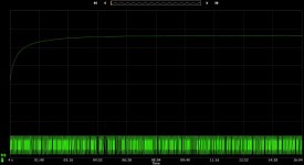
See 2SK170 plot and data attached.
Thanks DT
I have my lab notebook open here with thoughts in it.
Thermally conductive epoxy, you know glue the N and P FET’s together for common heat tracking.
Soldering vs push in solder-less Radio Shack style breadboard for heat stability
Tracking DC offset for an N and P pair vs time and temp. (So no I have not tested DC delta yet.)
There are other things on the list to test. Down the line the idea is compare cold pulse matched parts to parts matched over time in an operating temperature enclosure.
One thing that I have noticed:
Some FET’s with constant voltage applied drift up in Id current over time and increasing temperature. Example 2SK170.
Some FET’s with constant voltage applied drift down in Id current over time and increasing temperature. Example 2N5457.
Leads me to think that if an N and P pair are matched cold they my drift in opposite directions as they warm to operating temperature. (This is on my list to test)
See 2SK170 plot and data attached.
Thanks DT
Attachments
Last edited:
DT -- I can send you some "cold matched" 2N5460/2N5457 to put in the wigidizer.
Hello, jackinnj,
I’ll take you up on that.
It will make for a good test. You will know where we started with the “cold” numbers. There is a note on the ON Semiconductor 2N5457 Datasheet that addresses self-heating. Maybe it will make a difference matching N and P pairs or not. There is a similar note on the 2N5460 Datasheet, it does not say if IDSS goes up or down.
Note: Graphical data is presented for dc conditions. Tabular data is given for pulsed conditions (Pulse Width = 630 ms, Duty Cycle = 10%). Under dc conditions, self heating in higher IDSS units reduces IDSS.
Thanks DT
Hi Richard everyone
Just wanted to let you know the kit I built from jackinnj sound's great implemented into the output buffer for a Soha ii. I will get back later with some photos updates. Right now everything sits unboxed with just standoffs on the boards really messy but tremendous sound. This design has a lot of potential. BTW I'm an extreme novice with electronics and am amazed and grateful to everyone involved for the opportunity to build and use this great design.
Just wanted to let you know the kit I built from jackinnj sound's great implemented into the output buffer for a Soha ii. I will get back later with some photos updates. Right now everything sits unboxed with just standoffs on the boards really messy but tremendous sound. This design has a lot of potential. BTW I'm an extreme novice with electronics and am amazed and grateful to everyone involved for the opportunity to build and use this great design.
Hello Richard and All,
I have my lab notebook open here with thoughts in it.
Thermally conductive epoxy, you know glue the N and P FET’s together for common heat tracking.
Soldering vs push in solder-less Radio Shack style breadboard for heat stability
Tracking DC offset for an N and P pair vs time and temp. (So no I have not tested DC delta yet.)
There are other things on the list to test. Down the line the idea is compare cold pulse matched parts to parts matched over time in an operating temperature enclosure.
One thing that I have noticed:
Some FET’s with constant voltage applied drift up in Id current over time and increasing temperature. Example 2SK170.
Some FET’s with constant voltage applied drift down in Id current over time and increasing temperature. Example 2N5457.
Leads me to think that if an N and P pair are matched cold they my drift in opposite directions as they warm to operating temperature. (This is on my list to test)
See 2SK170 plot and data attached.
Thanks DT
Hi,
I do not recommend the -170 at all for this application. If you want to get the performance I did, you have to use only the devices at the current I used them. Otherwise, all bets are off.
If you do use the devices I chose for this project at the Id I used for matching, you should be at a zero TC (Temp Coeff) operating point.
I spent about $2000 USD on fets to measure and find the best one for my design criteria. It was no accident, the way it performs. For best results, you want dc and ac matched parts. DC matched at zero TC for no dc offset drift. IIRC, thats about 1 mA Id.
THx-RNMarsh
Last edited:
Hi Richard everyone
Just wanted to let you know the kit I built from jackinnj sound's great implemented into the output buffer for a Soha ii. I will get back later with some photos updates. Right now everything sits unboxed with just standoffs on the boards really messy but tremendous sound. This design has a lot of potential. BTW I'm an extreme novice with electronics and am amazed and grateful to everyone involved for the opportunity to build and use this great design.
Nice! You dont have to be an Rf engineer to have a stable wide bandwidth amplifier. Messy wiring/layout or not, it is very stable.
Enjoy your music! BTW --- what headphone brand/model are you using? Z?
THx-RNMarsh
Hi, I'm using the hifiman HE-4xx 35 ohm along with a es9028pro dac. I don't have any higher z phones to try but the 4xx do match well with this amps balanced sound signature. I will say this amp can take advantage of the best dac you can provide.
Hello All,
Here at the bench there is a bag of 500 Central 2N5457 JFETS. Looking at the Datasheet the min IDSS is listed at 1mA, the Max IDSS is listed at 5mA, and the typical IDSS is listed at 3mA.
I took a random 2N5457 JFET out of the bag and measured the IDSS at 2.37462mA. I checked a dozen or so additional JFETSs out of the bag and they seemed to group around 2.4 or 2.5mA Drain current. The test voltage was 12VDC on the freshly calibrated Keysight B2912A SMU. Both the source and gate were tied to ground or 0VDC. You know the typical way of testing Steady State Drain Current.
Wanting to stay close to the device matching methods outlined in the Linear Audio article I placed my randomly selected JFET in a test jig that looks like Figure 10 in the article. There is a 1K source resistor. As the current increased through the source resistor the gate to source voltage quickly became increasingly negative, exceeding -1.2VDC, the Vgs (off) voltage. I measured 123.100pA Drain current with the source resistor in place.
I did not find any JFET’s with lower Drain current (without the 1K resistor) to see if there is a sweet spot at -0.8Volts.
I know that I am in the weeds exploring part matching. This amplifier is exceptionally stable with very low distortion and very stable or completely missing DC drift without coupling capacitors.
Thank you Dr. Marsh.
Thanks DT
Hello,
Apologies
I posted results in error.
I pushed the wires into the incorrect location on the breadboard. Corrections are made.
Using Figure 10 in the Linear Audio article the Drain current measures 0.61196mA much closer to the 0.8 mA Drain current discussed by Dr. Marsh in his article.
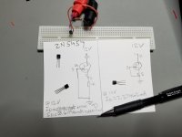
Including the 1K resistor in the test jig reduces the Drain current (IDSS) from 2.37462mA to a Drain current of 0.61196mA. See the attached photo of the test schematics and breadboard.
Thanks DT
Apologies
I posted results in error.
I pushed the wires into the incorrect location on the breadboard. Corrections are made.
Using Figure 10 in the Linear Audio article the Drain current measures 0.61196mA much closer to the 0.8 mA Drain current discussed by Dr. Marsh in his article.
Including the 1K resistor in the test jig reduces the Drain current (IDSS) from 2.37462mA to a Drain current of 0.61196mA. See the attached photo of the test schematics and breadboard.
Thanks DT
Attachments
Hello,
Apologies
I posted results in error.
I pushed the wires into the incorrect location on the breadboard. Corrections are made.
Using Figure 10 in the Linear Audio article the Drain current measures 0.61196mA much closer to the 0.8 mA Drain current discussed by Dr. Marsh in his article.
Including the 1K resistor in the test jig reduces the Drain current (IDSS) from 2.37462mA to a Drain current of 0.61196mA. See the attached photo of the test schematics and breadboard.
Thanks DT
😎 🙂
-RNM
I am looking for a Mouser bill of material to order all my part's from there. Has anyone done one up for this project? Please share would give me one less thing to get done to make this build.
I am looking for a Mouser bill of material to order all my part's from there. Has anyone done one up for this project? Please share would give me one less thing to get done to make this build.
Have a word with https://www.diyaudio.com/forums/members/jackinnj.html
min order of 2500 for
610-2N5460 at Mouser, same for Digi-key, off to ebay? polida2008 has some, I have bought from them, seem to be okay
610-2N5460 at Mouser, same for Digi-key, off to ebay? polida2008 has some, I have bought from them, seem to be okay
The second set of boards I burned can accomodate SMT devices, as well as the pinout for J74/K170
Jameco has the originals, still. Probably a good idea to snap up 100 or so.
Thanks for the heads-up, Jan. I ordered 100 pieces of each (2N5457, 2N5460) and they were delivered this morning.
Thanks for the heads-up, Jan. I ordered 100 pieces of each (2N5457, 2N5460) and they were delivered this morning.
Check them out with a curve tracer and some Fairchild or OnSemi (Motorola) originals.
The batch of 2N5457 I bought from them were rebranded --
That is strange, Jameco is a bona fide outfit. Maybe they were ripped off too ...
I would actually go to their store when they still had one, must have been last century.
Jan
I would actually go to their store when they still had one, must have been last century.
Jan
Hello,
A couple of months ago I renewed the effort looking at the magic of FET’s and Dr Marsh’s headphone amplifier.
A month or so ago I bought 100 of each 2N5457 and 2N5460 from Jameco. These JFET’s labeled “Fairchild” did not look right when tested on the bench. If I recall correctly it was the 2N5460 that was way off and not looking like the datasheet. The IDSS was well below the 1mA minimum called out on the datasheet. The Id Vg curves (Drain current and gate Volt curves) did not look like the datasheet either. These JFET’s from Jameco are set aside on the bench top for later.
Too much fun!
DT
- Home
- Amplifiers
- Headphone Systems
- Marsh headphone amp from Linear Audio