@hellokitty,
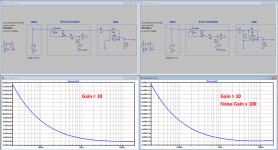
As Promised, I show you how a well behaving EC handles noise. I made a relatively simple EC circuit with an Op-Amp having much lower noise as the LT1364 has, to show you that the noise from the LT1364 will be cancelled by the EC, and only the own noise from the EC will remain.
I have made 4 sims, resp. with a gain of 10, as in your original circuit and also with a gain of 1, in both cases without and with a 10 Ohm resistor between the inputs to raise the noise.
As long as your EC cannot produce exactly identical noise spectra for all these 4 configurations, I find it very hard to believe that your EC is working properly and therefore most likely will not meet the distortion figures that you are expecting.
Hans
Attachments

Nice layout! I read about Cherry's 8-shape, great that you managed to improve it further.
What kind of distortion do you achieve with this layout? Is the input balanced or single-ended? I presume the big capacitors are the power supply capacitors rather than local decoupling, is that correct?
The PCB is the output stage only. About 0.1% distortions @20KHz @ 500W/4ohm open loop. With an ULGF of about 1MHz (two pole compensation) and 40dB of NFB at HF, this is a 0.001% @20KHz @500W/4ohm and 0.0004% @20KHz @200W/8ohm amplifier. At 1KHz I didn't bother much, but everything is likely under 0.0001%. Not to shabby, if you ask me.
Distortions are 90% 3rd harmonic residuals. This proves that most of the magnetic induction distortions are gone (they are typically 2nd harmonic).
The two pole compensated front end is single ended, but a balanced input front end is not a big deal, I don't see this as required though.
The big caps are 1000uF/80V @ 105C, one per each output device (total of 2x5,000uF), they are bypassed by SMD ceramics on the bottom layer. No, these are only to resolve the high currents on the board, the power supply has separate 2x27,000uF/80V, probably an overkill, but this is what Mouser had on sale at that moment 😀.
As you also can see, no amortized output coil on the board, that is connected directly at the speaker terminal. To my experience, the output coil is an endless source of magnetic trouble when installed on the PCB and the reason why I cringe when I see a claimed 0.000x% distortion amplifier with a PCB coil radiating straight to the input stage. That's simply simulation BS.
And no, I'm not looking for investors
 .
.
Last edited:
How do you keep the connection to the power supply from radiating? By keeping high audio frequency currents on board using damped series inductors, like Cherry?
How do you keep the connection to the power supply from radiating? By keeping high audio frequency currents on board using damped series inductors, like Cherry?
Yes.
I made a typo in the above noise image having a gain = 1.
The mentioned noise gain increase with the added 10 Ohm resistor between the inputs of the LT1364 must not be 10x but 50x.
Hans
The mentioned noise gain increase with the added 10 Ohm resistor between the inputs of the LT1364 must not be 10x but 50x.
Hans
I made a typo in the above noise image having a gain = 1.
The mentioned noise gain increase with the added 10 Ohm resistor between the inputs of the LT1364 must not be 10x but 50x.
Guys, because all this debate happens in the simulation realm, did it occur to you that the LT1364 spice model has no provisions for modelling distortions? It is a behavioral macromodel, with a few diodes and a pair of mosfets (apparently some sort of limiter, which does not exist on the real chip). There are very few free op amp models correctly modelling the distortions, so the simulation based discussions about how much is the LT1364 distorting, and how much is EC lowering those distortions, are not even theoretical; from a real world perspective they are simply bollocks, way before entering the anyway shaky -150dB grounds.
Okay well, I appreciate the help from everyone.
But at this point I am repeating myself too much.
Let's just all admit that I am stupid and my circuit sucks and call it a day.
I'm going to make my black box and get it measured as suggested.
But at this point I am repeating myself too much.
Let's just all admit that I am stupid and my circuit sucks and call it a day.
I'm going to make my black box and get it measured as suggested.
 Let's just all admit that I am stupid and my circuit sucks and call it a day.
No, way, you made many laugh, now you go build that circuit and make it work

And make that black box with strings of series-connected equal resistors for the gain setting resistors, and with a layout that minimizes magnetic crosstalk from the supply-output stage-supply loop to the inputs and outputs, and see where you end up.
There are quite a few things that LTSpice cannot do in a reliable way, but when in a simulation an EC design is not able to control noise in a believable way, which seems to be the case here, distortion modelling of a certain component is completely irrelevant. ��Guys, because all this debate happens in the simulation realm, did it occur to you that the LT1364 spice model has no provisions for modelling distortions? It is a behavioral macromodel, with a few diodes and a pair of mosfets (apparently some sort of limiter, which does not exist on the real chip). There are very few free op amp models correctly modelling the distortions, so the simulation based discussions about how much is the LT1364 distorting, and how much is EC lowering those distortions, are not even theoretical; from a real world perspective they are simply bollocks, way before entering the anyway shaky -150dB grounds.
And don’t we all agree that simulating beyond -120dB is wishfull thinking.
Hans
Marcel, this probably deserves a separate topic, but the magnetic effects of the half rectified power supply currents can be largely avoided by a clever PCB layout. Find attached such a layout I developed for a high power (up to 500W/4ohm) amplifier using Thermaltrak devices to compensate for temperature.
This is based on an idea from the same Cherry paper you quoted, where he suggested an "8" shape input stage layout to avoid magnetic effects. Here, the idea is to alternate npn and pnp devices and drag the +/- power supply lines through the middle of the PCB on both sides. This is equivalent to twisting the power supply lines straight from the power devices pins, the resulting external magnetic field being essential sinusoidal (much less harmonics than a full rectified sine), and I can vouch the practical results are nothing but spectacular compared to the standard layout with +/- supply lines each at the edge of the PCB.
As you can also see from the attached photo, the output trace takes the edges of the PCB, with the feedback pickup nicely placed at the current centroid.
Of course, this has nothing to do with -290dB distortions, but my result shows that such a layout can help not only in reducing the output stage magnetic distortions (such distortions cannot be in principle reduced by increasing the loop gain) but also making the whole problem of wiring a power amp much less critical.
I have no idea why such a layout was never employed in any commercial products (to the extend of my knowledge) since it is essentially a free method to improve performance. It probably doesn't sound good enough for the audiophiles 😀
Very nice layout! You put me to (re)thinking things I thought were obvious ...
Jan
Let's just all admit that I am stupid
Not at all. Ignorance can easily be rectified, and we all see you're working on it.
Stupidity would haunt you until eternity ;-)
Jan
Quite a few of us have spent their time to support you, helping to let your feet landing on realistic solid ground. A more mature reaction would be to come with a reasoning why your EC does not treat noise the way one would expect, or going back to the drawing board to see if something is not designed properly.Let's just all admit that I am stupid and my circuit sucks and call it a day.
I'm going to make my black box and get it measured as suggested.
Hans
Loved to see the course of events if the thread starter would be from Russia.Quite a few of us have spent their time to support you, helping to let your feet landing on realistic solid ground.

Syn08/Marcel,
I took a look at the Cherry paper. Clear that by laying the supply tracks on top of each other along with the speaker output will reduce the loop areas and mutual coupling. But, in Fig3 of his paper, he shows the speaker output coming out next to the amplifier input.
This seems to defy all the advice dished out to amplifier designers.
I normally group the 0V, supply pins, and speaker output together where they enter the board to keep the loop areas as small as possible.
I get Cherries figure of 8 idea, but not the input next to the speaker output.
Any comments from your side?
Loved to see the course of events if the thread starter would be from Russia.
You mean the poster's reactions to our comments would be very different? ;-)
Jan
Syn08/Marcel,
I took a look at the Cherry paper. Clear that by laying the supply tracks on top of each other along with the speaker output will reduce the loop areas and mutual coupling. But, in Fig3 of his paper, he shows the speaker output coming out next to the amplifier input.
This seems to defy all the advice dished out to amplifier designers.
I normally group the 0V, supply pins, and speaker output together where they enter the board to keep the loop areas as small as possible.
I get Cherries figure of 8 idea, but not the input next to the speaker output.
Any comments from your side?
No, except that most amplifiers have the input and output connectors on the same side (the back panel), so you need to route the output signal to the same side as the input somehow. Besides, you need to connect it to the feedback network, which will usually be close to the input as well.
I never tried Cherry's layout advice myself, so syn08 may be better at answering your question.
Quote:
Originally Posted by hellokitty123 View Post
Let's just all admit that I am stupid
To each his own but I don´t see this "admission" as a true one, just a typical temper tantrum, or kicking the chess table after failure to win.Not at all. Ignorance can easily be rectified, and we all see you're working on it.
Stupidity would haunt you until eternity ;-)
Jan
"We" are left with a bitter taste in the mouth ... or at least that´s the intention.
Just sayin´
Quote:
Originally Posted by Lazy Cat View Post
Loved to see the course of events if the thread starter would be from Russia.
Well, short ago (1 - 2 Months?) a Russian or Ukrainian Forum Member posted some "extreme" ideas, and presented as "proof" a few "papers" ... all in Russian language and no translation was ever offered.You mean the poster's reactions to our comments would be very different? ;-)
Jan
It didn´t exactly help his cause that he became quite exasperate and angry to begin with and even less when he admitted "Russian Scientists want to kick me" or some similar action.
So yes, your doubt is answered 🙂
Inputs and outputs on the same side or not ?
Many PCB design put them on opposite side, as to mimick the schematic or fear of coupling.
PCB designer should think about the outside cabling to use the PCB.
I think the better way is inputs and outputs at the same side. That gives an overall U routing on the PCB.
Many PCB design put them on opposite side, as to mimick the schematic or fear of coupling.
PCB designer should think about the outside cabling to use the PCB.
I think the better way is inputs and outputs at the same side. That gives an overall U routing on the PCB.
No, except that most amplifiers have the input and output connectors on the same side (the back panel), so you need to route the output signal to the same side as the input somehow. Besides, you need to connect it to the feedback network, which will usually be close to the input as well.
I never tried Cherry's layout advice myself, so syn08 may be better at answering your question.
I think although the connectors are located on the back panel, they are probably separated on the PCB in most amplifiers - as on opposite sides of the board or well away from each other.
I would say my current layouts are like a '=::=' in that power, GND and speaker all come into together, then I run the ground and the + or - supply rail over the ground ('=') to the output devices and localized decoupling which are either side of where the inputs come in i.e. the '::' bit.
The input connection is on the lower side of the board off to one side.
Anyway, interesting to see Cherry's take on this.
- Status
- Not open for further replies.
- Home
- Source & Line
- Analog Line Level
- -290 dB Distortion?