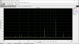
Sorry guys, attached is the correct 10kHz -40dBfs spectrum, apologies for the mistake.Nasty things come at higher frequencies, but there is no analog reconstruction filter at the DAC output. 6kHz -20dBfs, 10kHz -40dBfs, 10kHz -60dBfs.
Attachments
Hi John (EC Designs)
What are your thoughts of a Balanced version of your I2S to Sign Magnitude ??
What are your thoughts of a Balanced version of your I2S to Sign Magnitude ??
Hi Sven257,
It is very easy to construct a balanced TDA1541A DAC using the Sign Magnitude decoder circuit I posted earlier. You will need 4 x TDA1541A for that and you have to use the simultaneous interface setting (pin27 connected to -5V):
Chip #1 receives DL-, DL+ (DL, DR)
Chip #2 receives DL+, DL- (DL, DR)
Chip #3 receives DR-, DR+ (DL, DR)
Chip #4 receives DR+, DR- (DL, DR)
The advantage of a DAC with true balanced output is that you can double the output signal amplitude and you can cancel common mode noise.
What are your thoughts of a Balanced version of your I2S to Sign Magnitude ??
It is very easy to construct a balanced TDA1541A DAC using the Sign Magnitude decoder circuit I posted earlier. You will need 4 x TDA1541A for that and you have to use the simultaneous interface setting (pin27 connected to -5V):
Chip #1 receives DL-, DL+ (DL, DR)
Chip #2 receives DL+, DL- (DL, DR)
Chip #3 receives DR-, DR+ (DL, DR)
Chip #4 receives DR+, DR- (DL, DR)
The advantage of a DAC with true balanced output is that you can double the output signal amplitude and you can cancel common mode noise.
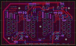
UPDATED DUAL TDA1541A PCB
I have almost finished the few modifications to my original pcb with the following changes:
NO SMD PARTS except the optional UFL sockets.
Jumpers to change from TWC to Simultaneous mode.
Pins for connecting battery power to each dac power pin directly.
Stacking of the boards with the upper pcb being the 'master' supplying data and power inputs, and signal outputs linked by long pin strips and sil sockets on the underside. (may be useful for a balanced ECD Signed Binary configuration)
U.FL pads added for direct connection to data source eg IanCanada's I2S-PCM board.
-15V regulator moved closer to the dac pin.
You can of course use external power by linking the in and out pads of the regulators.
Jumper to link pin 16's of the Dacs'
Low frequency dem clocking (with ECD's permission.) designed for 3.5mm pitch Nichicon UFL very low leakage capacitors.
Provision for small inductor, ferrite bead or low value resistor (10r) in the supply to each power pin.
Provision for low value resistor (eg 33r) in the data lines .
The dacs are separate and do not share data lines and there is no on board I/V.
Board size is 150 x 90mm 1.6mm FR4
Available in about 3 - 4weeks Please pm if interested and I will post a group buy. Price will be my cost price + postage & packing.
Attachments
Last edited:
Hi Batteryman,
Looks good. I could use it for my I2S board
A few comment if I may:
It could be hard to the to the DA SD UFLs at CN2R between the caps.
It would be easier for interconnection to have all UFL's in line parallel to the top or bottom edge
Looks good. I could use it for my I2S board
A few comment if I may:
It could be hard to the to the DA SD UFLs at CN2R between the caps.
It would be easier for interconnection to have all UFL's in line parallel to the top or bottom edge

Hi Batteryman,
Looks good. I could use it for my I2S board
A few comment if I may:
It could be hard to the to the DA SD UFLs at CN2R between the caps.
It would be easier for interconnection to have all UFL's in line parallel to the top or bottom edge
I will look into that, but best to fit the UFL connectors first.
I use it with an IanCanada I2S to PCM converter because this has various advantages:
Iancanada's products are here:
GitHub - iancanada/DocumentDownload: Download documents of Ian's products
a) Balanced outputs - one dac is for the left channel and the other, the right.
This is the best and correct way of implementing balanced output. You can then connect a transformer across the outputs (100r I/V resistors on each output) without worrying about the 2ma offset, as I do. (whether you inject current to cancel this is up to you but I don't like the sound - its too cold & clinical)
b) Stops the clock after latching.
c) Simultaneous mode is used.
d) Optional U.FL ouput connectors
I do also use his Fifo II and clock board because the Fifo can accept other data formats than I2S. It also has two I2S inputs so one for CD, and one for USB (using a £10 usb-I2S adaptor)
Last edited:
Here what I mean - it would be difficult to fit UFLs this way.I will look into that, but best to fit the UFL connectors first.

I have all of Ian's boards 😉
Would anyone be interested in Gerbers/code for an I2S to PCM board based on a $3 MachX02 FPGA?
It's designed as a pin-compatible replacement for the SAA7220 and generates its own 3.3V supply from the 5V pin. Inputs and output data lines are 3.3V LVCMOS (LVTTL) compatible, which works well with the TDA1541A. Obviously, one could use it in whatever design they wanted. Programming is easy, as it works on the same principle as the TinyFPGA boards.
By design it should work fine up to 384kHz or just above as it divides the BCLK by 4 during operation.

Output:

No worries about the LSB on this one. LE is clocked on the falling edge of the LSB clock tick and the bits are toggled on the rising edge providing plenty of setup and hold time for the TDA1541 to take the bits.
It is a direct implementation of the datasheet specifications.
It's designed as a pin-compatible replacement for the SAA7220 and generates its own 3.3V supply from the 5V pin. Inputs and output data lines are 3.3V LVCMOS (LVTTL) compatible, which works well with the TDA1541A. Obviously, one could use it in whatever design they wanted. Programming is easy, as it works on the same principle as the TinyFPGA boards.
By design it should work fine up to 384kHz or just above as it divides the BCLK by 4 during operation.
Output:
No worries about the LSB on this one. LE is clocked on the falling edge of the LSB clock tick and the bits are toggled on the rising edge providing plenty of setup and hold time for the TDA1541 to take the bits.
It is a direct implementation of the datasheet specifications.
Last edited:
SAA7220 replacment
Hi raptorlightning, this sounds quite interesting. So one could swap its SAA7220 vs this board in any 1541 CD player and with some modification, a forth i2s wire and swith TDA to PCM it became a NOS PCM CD player. Is it so simple? If yes, I would be interested! Soldering the FPGA might be a pain?
Cheers
Ernst
GB for the PCB?
Soldering the FPGA shouldn't be the problem, just pre-solder the pads, a small dot of epoxy beneath the IC and the use of hot air or an oven.
Soldering the FPGA shouldn't be the problem, just pre-solder the pads, a small dot of epoxy beneath the IC and the use of hot air or an oven.
GB for the PCB?
Soldering the FPGA shouldn't be the problem, just pre-solder the pads, a small dot of epoxy beneath the IC and the use of hot air or an oven.
Do not use any epoxy, just solderpaste and it will work perfectly. Or if you use regular solder still dont use epoxy. If you reflow the solder the chip will move exactly into the right position.
Would anyone be interested in Gerbers/code for an I2S to PCM board based on a $3 MachX02 FPGA?
It's designed as a pin-compatible replacement for the SAA7220 and generates its own 3.3V supply from the 5V pin. Inputs and output data lines are 3.3V LVCMOS (LVTTL) compatible, which works well with the TDA1541A. Obviously, one could use it in whatever design they wanted. Programming is easy, as it works on the same principle as the TinyFPGA boards.
By design it should work fine up to 384kHz or just above as it divides the BCLK by 4 during operation.
Output:
No worries about the LSB on this one. LE is clocked on the falling edge of the LSB clock tick and the bits are toggled on the rising edge providing plenty of setup and hold time for the TDA1541 to take the bits.
It is a direct implementation of the datasheet specifications.
As far as I can see , you use a continuous clock. Both Ians and Ryans version uses stopped clock operation to lower jitter and noise.
Do not use any epoxy, just solderpaste and it will work perfectly. Or if you use regular solder still dont use epoxy. If you reflow the solder the chip will move exactly into the right position.
Yeah, I agree, without the "feeling" what is too much, standard epoxy can create a real mess. I mean a really tiny dot of epoxy, as epoxy is shrinking while hardening. Of course, the much more appreciable solution is to use solder paste.
Hi, I would be interested in the code.
I tried the same thing about 2 years ago, but without good result. Would love to continue this project again soon!
I tried the same thing about 2 years ago, but without good result. Would love to continue this project again soon!
Would anyone be interested in Gerbers/code for an I2S to PCM board based on a $3 MachX02 FPGA?
It's designed as a pin-compatible replacement for the SAA7220 and generates its own 3.3V supply from the 5V pin. Inputs and output data lines are 3.3V LVCMOS (LVTTL) compatible, which works well with the TDA1541A. Obviously, one could use it in whatever design they wanted. Programming is easy, as it works on the same principle as the TinyFPGA boards.
By design it should work fine up to 384kHz or just above as it divides the BCLK by 4 during operation.
Output:
No worries about the LSB on this one. LE is clocked on the falling edge of the LSB clock tick and the bits are toggled on the rising edge providing plenty of setup and hold time for the TDA1541 to take the bits.
It is a direct implementation of the datasheet specifications.
As far as I can see , you use a continuous clock. Both Ians and Ryans version uses stopped clock operation to lower jitter and noise.
I'm not sure if that is feasible at 384kHz. You can't run the bit clock higher than 6.4MHz (according to the datasheet) and this method runs it right at the maximum (24.576MHz/4 = 6.144MHz). The latching process occurs during a clock null, and you must eventually clock in the next words, which requires toggling the clock. The data must flow or it will underrun the incoming data. I don't see how stopping it would really affect the amount of noise in the long run - you have to toggle the clock eventually.
Jitter depends entirely on your source clock quality. There is no reclocking done with this board. It is just a sea of gates, clocked by the incoming bit clock stream.
Last edited:
Hi, I would be interested in the code.
I tried the same thing about 2 years ago, but without good result. Would love to continue this project again soon!
I'm glad there's some interest. I've attached a zip that includes the following:
- Another zip with the Gerber files prepared for OSHPark or another PCB fab
- The SystemVerilog code for conversion. The top-level instantiation module ends in *_fpga.sv. The LPF file is for pin definition.
- Schematic
- Bill of Materials
- Image ready to flash with the TinyFPGA Programmer utility in JED format.
I'm not sure if there's a need for a GB. It's $4.75 for 3 boards shipped from OSHPark...
As far as soldering goes, this project does require SMD soldering, and the 32QFN package may be intimidating to beginners. Unfortunately our hobby must adapt to the times as some of the best new devices are only coming in SMT packages.
For soldering SMT devices, my best advice is magnification, lots of good flux, and a steady hand. The QFN package can be soldered just like a SOIC - apply solder to one corner pad, align the device on all 4 sides, and tack it down, then tack it on an opposing pin. For the rest of the pins, if you have enough flux, you should be able to easily drag solder across the sides leaving no bridges and soldering every pin with just a stroke.
Note: I haven't tried the DEM clock. So... user beware on that one if you decide to recompile the code in Lattice Diamond, but I don't see why it wouldn't work.
Attachments
Last edited:
I am not sure you have been reading this thread very thoroughly, as there has been much talk about the benefits of stopped clock operation and of how many things influences the performance of the TDA1541A. Jitter is not only a a matter of clock entering the TDA1541 is low jitter, but the uncertainty (timewise) by witch TDA1541A converts the stored data to the analog out put.I'm not sure if that is feasible at 384kHz. You can't run the bit clock higher than 6.4MHz (according to the datasheet) and this method runs it right at the maximum (24.576MHz/4 = 6.144MHz). The latching process occurs during a clock null, and you must eventually clock in the next words, which requires toggling the clock. The data must flow or it will underrun the incoming data. I don't see how stopping it would really affect the amount of noise in the long run - you have to toggle the clock eventually.
Jitter depends entirely on your source clock quality. There is no reclocking done with this board. It is just a sea of gates, clocked by the incoming bit clock stream.
Here is just a few comments from ECdesign on these matters, and I recommend you read much more of the thread to look into his observations and measurements.
Post 6101 there is a little about the noise when the clock is active
Post 6126 you can see the timing of the stopped clock operation.
It has nothing to do with sampling frequency. The timing is the same even though the CLK is 384 Khz. The main feature is that at the time the LE goes high, there is NO activity on any of the DATA or CLK inputs.
I am not the right one to explain it correctly, look for ECdesigns explanations.
Last edited:
- Home
- Source & Line
- Digital Line Level
- Building the ultimate NOS DAC using TDA1541A