I really think that your stand of refusing to add pictures when everyone has asked for them (and even pasted links to instructions on how to upload them freely to the server) is going to limit the amount of help people can give you and, quite frankly, limit your own chances of finding a quick and painless solution.
Please, instead of investing more time into doing potentially more damage, invest time in posting some pictures so people can help you as your beautiful amp deserves!
Rafa.
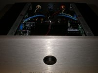
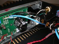
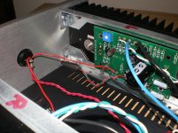
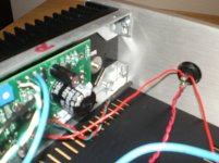
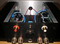
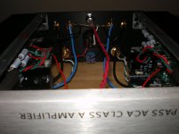
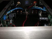
Rafa, Here are some pics:
")
Attachments
-
 IMGP0068.jpg435.5 KB · Views: 434
 -
 IMGP0069.jpg507 KB · Views: 419
 -
 IMGP0070.jpg604.9 KB · Views: 242
 -
 IMGP0071.jpg628.4 KB · Views: 227
 -
 IMGP0072.jpg591.4 KB · Views: 219
 -
 IMGP0073.jpg621.7 KB · Views: 170
 -
 IMGP0074.jpg605.9 KB · Views: 173
 -
 IMGP0075.jpg546.5 KB · Views: 187
 -
 IMGP0077.jpg417 KB · Views: 163
 -
 IMGP0076.jpg406.1 KB · Views: 174
I cannot spot anything obvious, I'm sure others will be of more help.
I have one question: are you able to see perpendicular into the PCBs to make sure that no cable or component leg is touching the heatsink from the non-component side? If one of those cables is too long it could be making contact with the heatsink.
That would be the first thing I would try to check.
Best,
Rafa.
I cannot spot anything obvious, I'm sure others will be of more help.
I have one question: are you able to see perpendicular into the PCBs to make sure that no cable or component leg is touching the heatsink from the non-component side? If one of those cables is too long it could be making contact with the heatsink.
That would be the first thing I would try to check.
Best,
Rafa.
Hard to see perpendicular, tried it, but I am sure no cables are in contact with heatsink.
Thanks
You need to connect the meters black lead to the main zero volt (ground point) which is that common 'bussbar' connection at the back of the amp.
Make sure your meter is on DC volts and check the supply voltage on the middle leg of Q2 which should be 24 volts.
You should also have 24 volts on one end of R7.
Those are the first things to check.
Make sure your meter is on DC volts and check the supply voltage on the middle leg of Q2 which should be 24 volts.
You should also have 24 volts on one end of R7.
Those are the first things to check.
Problem with ACA 1.6: Q2 23.V, won't bias
Yesterday I finished my ACA 1.6, standard stereo configuration.
All went well, but when I hooked it up the right channel played much softer than the left. Tried some other speakers, same situation.
Now this morning I started trouble shooting, and found on the RHS board
- the center pin of Q2 reads 23.7V, whilst Q1 reads 12.04V after biasing
- Q2 stays on 23.7V, does not react to turning the potentiometer.
Can anyone give me some pointers where to look?
For full information, I first installed Q4 and Q3 the wrong way around (rushing...), took them off the boards and but them back the right way. Would damage to these transistors lead to the fault I am experiencing?
Thanks in advance,
Laurens
... on the RHS board
- the center pin of Q2 reads 23.7V, whilst Q1 reads 12.04V after biasing
- Q2 stays on 23.7V, does not react to turning the potentiometer.
...
That is correct. The centre pin of Q2 (the Drain) is fixed to the +24 volt supply and cannot change.
The centre pin (Drain) of Q1 will change as you move the pot P1 and 12 volts is spot on.
Did you 'switch on' with Q3 and 4 the wrong way round?
Have you tried swapping left and right inputs as well yet?
Alan
Attachments
Last edited:
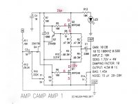
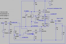
ACA measurement points
Boyz , for troubleshooting purposes , always include some measurements , information of exact schematic (few schm. iterations are there) to be sure about nomenclature , and few well made pictures
example of important measurement points , you can use it as general guide (parts nomenclature not by Papa's schematic!!):
Attachments
You could measure voltages on the good board and check it on the bad board. Check also resistor values. Value R11/R12 correct?I first installed Q4 and Q3 the wrong way around (rushing...), took them off the boards and but them back the right way. Would damage to these transistors lead to the fault I am experiencing?
Laurens
Hi Alan4411,
Thanks for confirming that Q2 is OK.
I turned Q3 and Q4 around before powering, but i was afraid they might have gotten too hot from soldering/desoldering/resoldering.
As per your advice, I switched inputs, output and pre-amp, but every time it is the RHS board that gives low output.
Hi EddyvdB,
Yes, I will do a L / R comparison to find where the problem is. Probably touch up some solder points as well, just to make sure.
I will report my findings here, any pointers will be appreciated.
Cheers,
Laurens
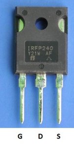
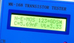
I think this little transistor tester is very useful for DIY people.
It automatic finds out which device it is (FET, Bipolar, Diode, Resistor, Capacitor etc.) and it does not matter how the wires are connected. It shows this in the display if the device is recognized. If the transistor is damaged it will be shown as "unknown or damaged" in the display.
In the example I test a IFRP250 (used for the MoFo). The display shows that it is a N type MOSFET. E is probably (Enhancement mode). Then it shows the Gate capacitance and the forward voltage to have it conducting (Vt). It also shows that wire 1 is G, 2 is D and 3 is S.
It is "made in China" so very cheap…….but useful and clever made I think. It is not for matching devices other than a very very raw match.
Attachments
Hi Zen Mod,
There is continuity between all pins on Q3 and Q4, so that would mean they are OK, right?
Hi Mooly,
I measured 0.501V (DC) on R4 and 0.500 on R5, so it would seem the problem is on R10 / R11 or R12.
I will take both boards from the case so I can see what I am doing.
Thanks for all your help so far.
There is continuity between all pins on Q3 and Q4, so that would mean they are OK, right?
Hi Mooly,
I measured 0.501V (DC) on R4 and 0.500 on R5, so it would seem the problem is on R10 / R11 or R12.
I will take both boards from the case so I can see what I am doing.
Thanks for all your help so far.
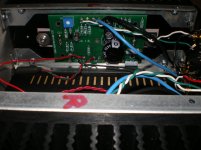
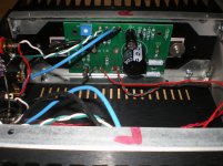
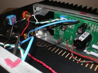
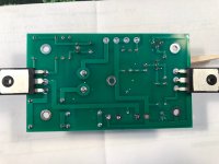
Rafa, Here are some pics:
Ed,
Thanks for the pics. Do you use a temperature controlled soldering iron (just curious), do you have a wet sponge or tip cleaner?
I see a number of areas that I would be suspicious of cold joints, lack of solder and too much solder. Just because there is a lot of solder doesn’t mean it thoroughly spreads into the hole. I would strongly recommend desoldering braid and liquid flux and addressing those problematic areas. In addition I am suspicious of the solder points in the input/output connections.
In particular, resistors R1-R4, I see a few that are suspicious. Notice how your voltage readings there are problematic.
I haven’t checked to see that you have the correct resistors populated in the proper locations, I am assuming so, since your voltages around the input JFET (Q4) and around the ZTX transistor (Q3) seem to be correct.
Best,
Anand.
Hi Zen Mod,
There is continuity between all pins on Q3 and Q4, so that would mean they are OK, right?
.....
well , there must be no continuity ........ it really depends of what you means by it
however , what I meant - check in situ that you don't have any shorts between transistor pins , showing that part is Dodo
in any case , compare readings with good channel parts , observing each time probes orientation (same orientation testing L against R channel parts)
BC,
All resistors, and Q3 and Q4 look correct. I am suspicious of a pin of Q1 that does not look shiny (pin closest to C4). I am also suspicious of the middle pin of Q2 (directly in series with R7). It also looks dull in the picture.
Add some flux if you can and resolder. Or reheat and resolder. Make sure your soldering iron is sufficiently hot if it is a temperature controlled type. I use 700 deg F or about 375 deg C.
And everything ZenMod said!
Best,
Anand.
Last edited:
- Home
- Amplifiers
- Pass Labs
- Amp Camp Amp - ACA