C237 was originally 15p, it was stable when I used MJL1302/3281
increased it to 22p, there was some peaking in the hi freq response, increasing C237 to 47p, removes this peaking, over compensated.
R13, I am not sure, does it force a lower input Z, 33K?
the printed schematic is in ltspice, you find my schematic hard to read?
Bypass R255 to control overshoot at the leading edges. I'm not sure why R13 is used.
Also, what are they up too sending the connection of R4 and R6 into the feedback signal? Isn't it positive feedback around the output stage to do so?
Hi Mark,
What if you put a 0.1uF capacitor between the collector and emitter of Q2?
Cheers,
Valery
Hi Valery
I'm using 100MHz fT transistors, no base stoppers, 100nF from rail to ground, no discernible oscillation. As I said before I used to use a 1k into the base of the reference transistor but stopped with no apparent ill effects.
Mark, the schematic of your lash up shows no return path from the CSS output to ground, except through the DMM, which will have a very high input resistance. Could that be a factor?
DMM resistance is 50 ohms. Burden voltage is 0.2V. At 4mA that's 50 ohms.
But don't get lost. The point is not, "setup B did not oscillate". The point is "setup A did oscillate". It's something that can happen in real life; it's something to guard against.
There was a thread contributor right here who said "I have never seen oscillation with the 2T shunt shunt current source and no base stopper resistors". My own tiny contribution is to say, I have seen oscillation and here are pictures of it. That person is welcome to ignore my measured data, of course.
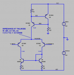
One application of this current source, is to provide tail current for a long tailed pair input stage. In this environment the current source is working into a very low impedance load, namely the emitters of the input transistors. Picture below.
What's the advantage to the current mirror? Differential balance. I guess I should ask what effect. Just tried it though. Lower THD at least.
Was there any sign of ringing on the CCS now?
Last edited:
Mark indirectly answer the question about R13 in my schematic, it defines the input R of the amp, since it is low Z node. Why terminate in the emitters vs ground is more the question? Maybe better RFI rejection?
The current mirror forces the balance of current in the 2 diff amps, thus the offset voltage. I thought I read in Bob Cordell's pwr amp book it affects 2nd order thd. But then again, some advocate that equal load emitter load resistors allow more headroom. There is no clear winner from what I am lead to believe. They had this discussion in Bob Cordell's power amp book thread.
The current mirror forces the balance of current in the 2 diff amps, thus the offset voltage. I thought I read in Bob Cordell's pwr amp book it affects 2nd order thd. But then again, some advocate that equal load emitter load resistors allow more headroom. There is no clear winner from what I am lead to believe. They had this discussion in Bob Cordell's power amp book thread.
(oops, realized i should move my post to the correct thread)
Hi Mark:
I share your concern. I've had one of these oscillate in the past also (without base stopper). I have learned over the years (the hard way when younger) to trust WaltJ's comments on such things.
I know you said you just use a different design now to avoid this - I'm just curious if you've noticed any connection/correlation between susceptibility and manufacturer ?
mlloyd1
Great point, mlloyd1! I had the same part# from two different manufacturers, on only two of the eight experiments.
BC550C: both Fairchild's and ON Semiconductor's device, oscillated
2N5401: both Fairchild's and ON Semiconductor's device, failed to oscillate
For the other six devices tested, I only had parts from one manufacturer.
BC550C: both Fairchild's and ON Semiconductor's device, oscillated
2N5401: both Fairchild's and ON Semiconductor's device, failed to oscillate
For the other six devices tested, I only had parts from one manufacturer.
Right - one of the important parameters with regards to probability of oscillation (besides the bandwidth, already noted) is hFE - the higher hFE -> the higher probability. 2N5401/5551 are rather safe.
BC550C is a much "better" transistor -> more dangerous...
2N5089 would also oscillate like hell...
BC550C is a much "better" transistor -> more dangerous...
2N5089 would also oscillate like hell...
Preventing oscillation
Hi Mark, I am reading a suggestion on oscillation prevention by an RF guy on the following web page:
Low Phase Noise Design: Common Emitter Transformer Feedback Buffer Amplifiers
..where it says, one technique to prevent CFP's from oscillating, is to select the driver transistor of much higher fT than the output transistor.
I am thinking here whether this technique is also applicable for the CCS compound discussed in this thread as well as they, the 2 transistors, work in a similar tight connection with each other.
I assume in your schematic that would be higher fT for Q2 and lower fT for Q1.
BC550C: both Fairchild's and ON Semiconductor's device, oscillated
2N5401: both Fairchild's and ON Semiconductor's device, failed to oscillate
For the other six devices tested, I only had parts from one manufacturer.
Hi Mark, I am reading a suggestion on oscillation prevention by an RF guy on the following web page:
Low Phase Noise Design: Common Emitter Transformer Feedback Buffer Amplifiers
..where it says, one technique to prevent CFP's from oscillating, is to select the driver transistor of much higher fT than the output transistor.
I am thinking here whether this technique is also applicable for the CCS compound discussed in this thread as well as they, the 2 transistors, work in a similar tight connection with each other.
I assume in your schematic that would be higher fT for Q2 and lower fT for Q1.
Thank you but I have abandoned this circuit; when you add the components to make it stop oscillating it has more parts than other current source circuits with higher performance. So I have chosen a different path. Other readers besides me, might find great benefit in the idea you suggest. Thanks for the recommendation!
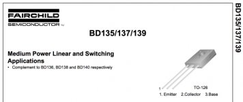
What it is with the BD139 and BD140 pinouts? EBC? ECB? WTF? BBQ?
ECB, with the legs downwards, facing the printing. Otherwise ICQ 🙂.Best regards!
What it is with the BD139 and BD140 pinouts? EBC? ECB? WTF? BBQ?
Kay Pirinha is correct, but in general - datasheet is your friend 😉 RTFM 😛
Attachments
Kay Pirinha is correct, but in general - datasheet is your friend 😉 RTFM 😛
The datasheet is what's throwing me off. Look at their pinout numbering. 321? So it's a bottom view? Or a typo? Who numbers from right to left? 🙄
Attachments
The datasheet is what's throwing me off. Look at their pinout numbering. 321? So it's a bottom view? Or a typo? Who numbers from right to left? 🙄

No, this is the top side with the markings.
See Figure 1:
3 = E
2 = C
1 = B
3-2-1 = E-C-B
Well, I agree - different manufacturers are showing the pinouts in different ways...
But there's always one truth 😀 They present the same thing in the end.
But there's always one truth 😀 They present the same thing in the end.
No, this is the top side with the markings.
See Figure 1:
3 = E
2 = C
1 = B
3-2-1 = E-C-B
I get that 3 2 1 are E C B but when the pinout numbering is backwards, you have to question. Or not, and design a board layout and order 500pcs just to realize you goofed up when it fries. 😛
- Status
- Not open for further replies.
- Home
- Amplifiers
- Solid State
- Bootstrapped amps. DX/Aksa/RCA/etc...