This is the PCB layout, where a female TE connector has to be placed on the PCB instead of Relay7 when using the 6 input GB board + Interface board.

Female PCB Connector is the :
TE CONNECTIVITY / AMP 2178710-8 Wire-To-Board Connector, Micro-MaTch Value-Line Series.
Enrico has already given the type number for a matching 130mm ribbon cable with a male connector for the VolCB side.
But 130mm might be a bit on the short side, so the 200mm version TE CONNECTIVITY 2205070-3 RIBBON CABLE might be better.
Hans
Hans,
I am looking in the PCB layout but I can't figure out how the TE connector can fit the R7 footprint. The pads for R2-3-4-5-6 can fit but not the R1 and the +5V.
Maybe I miss something?
Regards,
Enrico
I am looking in the PCB layout but I can't figure out how the TE connector can fit the R7 footprint. The pads for R2-3-4-5-6 can fit but not the R1 and the +5V.
Maybe I miss something?
Regards,
Enrico
Hans,
I am looking in the PCB layout but I can't figure out how the TE connector can fit the R7 footprint. The pads for R2-3-4-5-6 can fit but not the R1 and the +5V.
Maybe I miss something?
Regards,
Enrico
Hi Enrico,
Better double checked than not checked at all.
The yellow line shows how to the female connector will sit on the VolCB.
I think everything is O.K., including the mounting notch in brown on top.
Let me know if you still think something is wrong.

Regards,
Hans
Hi Enrico,
Better double checked than not checked at all.
The yellow line shows how to the female connector will sit on the VolCB.
I think everything is O.K., including the mounting notch in brown on top.
Let me know if you still think something is wrong.
View attachment 551143
Regards,
Hans
I fully agreed with you! Now looks OK but I will check again and let you know.
Thanks and Best Regards,
Enrico
I fully agreed with you! Now looks OK but I will check again and let you know.
Thanks and Best Regards,
Enrico
Now I see what caused the confusion, I had simply sent you the wrong picture.

Now I see what caused the confusion, I had simply sent you the wrong picture.
View attachment 551145
I was sure that you had rechecked! 🙂
For me, tested, and PnP is ideal 😀NATBERG, Lbud4 and pchw please review you choice specifying if you want only "bare board" or leave as it is if you want the boards done and tested.
Regards,
Enrico
Thanks!!
Forget to mention, the boards will be fully populated and tested unless you don't expressly ask for the bare board.
Fully populated would be excellent. yes please.
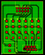
Interface PCB
I am done with the small PCB.
Hans, please give a look and let me know if there is something wrong... Thanks!
The board size is 48 x 38 mm. I can make a little smaller but I prefer to give some solid support to the 10 pin that will connect with the 6 input board.
As per the relay datasheet the protection diode is not required.
I will keep the list open for a while, there is no rush for this GB until the relevant Maja GB with the VolCB board is not ready.
Without saying, any comment or suggestion is welcome.
Best Regards,
Enrico
Attachments
This is the revised list after the design change
Please keep updated this list for any change, thanks.
emyeuoi - 2 PnP
NATBERG - 2 PnP
Lbud4 - 2 PnP
pchw - 2 PnP
badman - ? PnP
Please keep updated this list for any change, thanks.
emyeuoi - 2 PnP
NATBERG - 2 PnP
Lbud4 - 2 PnP
pchw - 2 PnP
badman - ? PnP
I'll take a tested PnP board- thanks for doing the heavy lifting (again!)
Thanks badman and well come back 🙂
Please give a look to my last post and update the quantity of boards you need.
Regards,
Enrico
Hi Enrico,I am done with the small PCB.
Hans, please give a look and let me know if there is something wrong... Thanks!
The board size is 48 x 38 mm. I can make a little smaller but I prefer to give some solid support to the 10 pin that will connect with the 6 input board.
As per the relay datasheet the protection diode is not required.
I will keep the list open for a while, there is no rush for this GB until the relevant Maja GB with the VolCB board is not ready.
Without saying, any comment or suggestion is welcome.
Best Regards,
Enrico
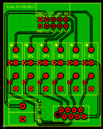
This must be the back side of the PCB.
Use the 9007-05-01 relay with built in suppression diode, which may be hard to get.
Or the 9007-05-00, which definitely needs a suppression diode (1N4148) to protect the PCF8574.
So I would advice adding the option of mounting a diode, just to stay universal.
Further everything seems O.K.
Hans
Hi Enrico,
This must be the back side of the PCB.
Use the 9007-05-01 relay with built in suppression diode, which may be hard to get.
Or the 9007-05-00, which definitely needs a suppression diode (1N4148) to protect the PCF8574.
So I would advice adding the option of mounting a diode, just to stay universal.
Further everything seems O.K.
Hans
Thanks Hans for the advise.
The 9007-05-01 are available in Mouser but you are right, this will make the board universal. I will add the pads in the bottom side.
Best Regards,
Enrico
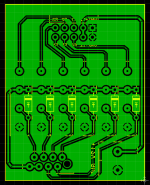
Now I'm a bit confused. I asked you in #134 whether this was the back side of the PCBHans,
Here is the revised board with the protection diodes added in the bottom side.
Best Regards,
Enrico
Now I get the impression that the side with the red dots is the component side.
In that case, the connector to the VolCB is mirrored.
See drawing below, from component side.

Hans
Now I'm a bit confused. I asked you in #134 whether this was the back side of the PCB
Now I get the impression that the side with the red dots is the component side.
In that case, the connector to the VolCB is mirrored.
See drawing below, from component side.
View attachment 551379
Hans
Hans,
Apologize for the confusion, I though you was referring to the side of the board where you suggest to install the diodes.
About the connector, the picture you shown is the footprint for the connector to be installed in the VolCB.
Looking at the datasheet of the cable (I can't post here now) the sideA (VolCB) and the sideB (soldered in the interface board) are mirrored. At least this is what I was able to figure out from the datasheets and the VolCB footprint you sent yesterday but maybe I am wrong
Anyway I will get one cable in the hands before to place the PCB's order to avoid any surprise
Thanks and Regards,
Enrico
Hi Enrico,Hans,
Apologize for the confusion, I though you was referring to the side of the board where you suggest to install the diodes.
About the connector, the picture you shown is the footprint for the connector to be installed in the VolCB.
Looking at the datasheet of the cable (I can't post here now) the sideA (VolCB) and the sideB (soldered in the interface board) are mirrored. At least this is what I was able to figure out from the datasheets and the VolCB footprint you sent yesterday but maybe I am wrong
Anyway I will get one cable in the hands before to place the PCB's order to avoid any surprise
Thanks and Regards,
Enrico
The documentation of the cable is a bit uncomplete, but your decision to buy one cable is the best way to proceed.
Regards,
Hans
- Status
- Not open for further replies.
- Home
- Group Buys
- Bruno Putzeys Preampli - GB for the 6 Input Board