Thanks! Should this variant be renamed FX9H? 🙂
I think it is compact enough for me to put two amps facing each other transistor-to-transistor on the same heatsink and maybe add a small fan 50mm to cool the heatsink.
I dont think APEX would object🙂 . Pl share the sch here, if I get time, I will make a layout for it.
Thanks! Should this variant be renamed FX9H? 🙂
I think it is compact enough for me to put two amps facing each other transistor-to-transistor on the same heatsink and maybe add a small fan 50mm to cool the heatsink.
This variant be renamed to FH9
I dont think APEX would object🙂 . Pl share the sch here, if I get time, I will make a layout for it.
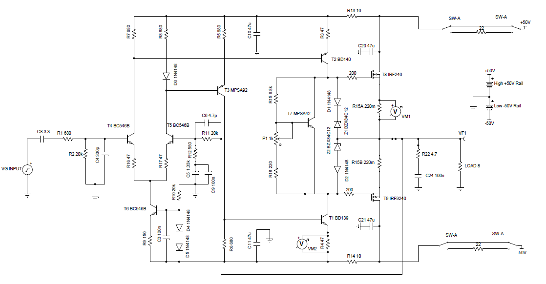
Here is the newly christened FH9 schematic from post 7228 but change Vbe multiplier MPSA42 to BD139 and have it mounted in between the two FETs on heatsink as temp sensor.
A new layout would be very nice. Thanks!
does anyone have a layout apex ax20 were tested ?
If yes, please share here
This AX20 are tested by me and work very well.
Regards
Attachments
Hello all indian diyer
I wanted to buy mje13007 and Mje5851
Please help me to find
If you have any contacts pls pm me
Thank you
I wanted to buy mje13007 and Mje5851
Please help me to find
If you have any contacts pls pm me
Thank you
Here is an idea for quick layout of FH9 modified from Fx-8.Here is the newly christened FH9 schematic from post 7228 but change Vbe multiplier MPSA42 to BD139 and have it mounted in between the two FETs on heatsink as temp sensor.
A new layout would be very nice. Thanks!
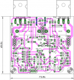
pl see for connection error. further optimization can be done,.
Attachments
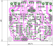
Here is an idea for quick layout of FH9 modified from Fx-8.
pl see for connection error. further optimization can be done,.
Sors and drain on IRFP9240 is reverted...
Here is an idea for quick layout of FH9 modified from Fx-8.
pl see for connection error. further optimization can be done,.
Thanks Prasi.
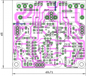
1. Can you move all BD139/140's close to end so all can be mounted on heatsink?
2. Can Q1&Q2 be adjacent so thermally tied together face to face and shrink tubed?
3. Yes, please check gate source and drain pin outs on IRFP240/9240.
4. I have not tested at 50v yet - I know several folks have mentioned that 50v may be too much?
Otherwise it looks great. Thanks
X
And;
If you want to use +-50vdc ,you must chance bd139-140 to mj340-350
Yes! Also try not to bias to high at 50V the one pair mosfet.
Why are you trying to run a single pair at 50v? Do you really believe you will hear the extra dB or two? All you're going to get is stressed devices for very little gain.
You are right and I was trying to get higher power out of them vs the lateral FETs. AndrewT did say that de rating to 75w (or 1/4 theoretical max) is best way to run them for higher reliability. 75w with 8ohms is only 25v - so how does one calculate what rail voltages are needed for a class AB? I currently have 35v rails - will that be enough? What is the calculation that is done and what assumptions are needed? 50% efficiency? So rails need to provide 150w? That would be 35v I think.
Thanks Prasi.
1. Can you move all BD139/140's close to end so all can be mounted on heatsink?
2. Can Q1&Q2 be adjacent so thermally tied together face to face and shrink tubed?
3. Yes, please check gate source and drain pin outs on IRFP240/9240.
4. I have not tested at 50v yet - I know several folks have mentioned that 50v may be too much?
Otherwise it looks great. Thanks
X
Ok, incorporated above changes. also supply to +/- 35V.
Attachments
Thank you Prasi! Very nice. I can't find anything wrong with it. Maybe others can also look too to verify.

Ok, incorporated above changes. also supply to +/- 35V.
You can rotate jumper J1 for 90deg and connect emiter and colector of two BD139 transistors (T1, T7)9...
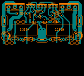
Hi Prasi, you can make this layout without jumper.
I have attached picture of components placement for upper side of your pcb.
Oh that's very nice. You are a true layout artist!
Thanks.
Why are you trying to run a single pair at 50v? Do you really believe you will hear the extra dB or two? All you're going to get is stressed devices for very little gain.
In fact one pair of lateral MOSFETs can easily run on +/-50V or even more. Elliott's P101 with one pair of lateral MOSFETs is designed to work at +/-56V (dual 40V secondaries transformer). P101 with two pairs is designed to work at +/-65-70V. Lateral MOSFETs are that robust! They have unique resilience to thermal runaway. Companies from UK are using them for 40 years exactly because that robustness and in most cases they even do not even require protection. It's very difficult to burn them even with prolonged hard work. But, of course, lower working voltages will provide almost absolute reliability in FX8 circuit.
Last edited:
Hi Prasi, you can make this layout without jumper.
I have attached picture of components placement for upper side of your pcb.
Hi Sonal,
Looking good!🙂. Pl go ahead and make the rest of the layout too, will be useful for builders.
here is a jumper-less version based on my earlier version. I am not able to find time😱.
reg
Prasi
Attachments
- Home
- Amplifiers
- Solid State
- 100W Ultimate Fidelity Amplifier