I did a DC check using a pair of bc182b (hFE ~270)
@ ~20V to ~30V across the CCS I found ~ 900k effective resistance/impedance.
But it did not change instantly as the new load was applied. It drifted pretty slowly to the new value of Iccs. and drifted slowly back to the previous Iccs when the load reverted.
Thinking this was a temperature effect in the upper transistor, I added a cascode with the voltage between the two set with a green LED.
Now the change in voltage is seen by the cascode and the CCS transistor sees a nearly constant Vce.
Now the effective resistance (measured ~400k) drifted from old value to new value just as slowly, but more consistently. The cascode appeared to have lowered the impedance and did not remove, nor attenuate the supposed temperature effect.
I did a DC check using a pair of bc182b (hFE ~270)
@ ~20V to ~30V across the CCS I found ~ 900k effective resistance/impedance.
But it did not change instantly as the new load was applied. It drifted pretty slowly to the new value of Iccs. and drifted slowly back to the previous Iccs when the load reverted.
Thinking this was a temperature effect in the upper transistor, I added a cascode with the voltage between the two set with a green LED.
Now the change in voltage is seen by the cascode and the CCS transistor sees a nearly constant Vce.
Now the effective resistance (measured ~400k) drifted from old value to new value just as slowly, but more consistently. The cascode appeared to have lowered the impedance and did not remove, nor attenuate the supposed temperature effect.
This is odd and beyond my comprehension Andrew, hopefully someone else has a better idea about what's going on with your circuit.
Gordon.
Returning briefly to the theme of test equipment accuracy and calibration, I picked up the latest copy of EPE magazine today when in town with my eldest daughter. Amongst others, the magazine featured a project for a 10 V +/-0.05% voltage reference based on an AD 587 chip. Great thing is you get this accuracy as is without the need for calibration that would involve a 6&1/2 digit meter! If you do have access to such a meter you can achieve +/-0.0002% accuracy from this device!
Gordon.
Gordon.
Last edited:
Another very frustrating day trying to refine my setup to minimize the issues identified in post #200. First tried using 7812 & 7912 voltage regulators in an attempt to clean up the output of the bench PS, they actually made matters a lot worse, putting out around 800uV peak to peak broadband noise! Perhaps lm317 / 337 would be better? Or perhaps a capacitance multiplier.
Have resolved the DC offset problem by 1. Changing the capacitor that couples the CCS sense resistor to the amplifier to a tantalum cap instead of an electrolytic. 2. By AC coupling the 2 amplification stages.
The noise and interference pickup from the -ve rail has been improved by returning the CCS sense resistor to ground, however this requires a slightly odd power supply arrangement, namely +25 / -15 volts as the ne5532 cannot take more than 44 volts. My intention had been to supply the CCS from a + 30 v rail and the amplifier with +/- 12 or +/- 15 volts with local voltage regulators, but the noise output of these has pushed me to scrap that idea.
Using just the original RC power supply filters and returning the sense resistor to ground has made a considerable improvement as well as more vigilance over layout, such as putting the amplifier physically close to the CCS sense resistor and keeping the path of the stimulus from the signal generator away from the amplifier input. I think now there may be light at the end of the tunnel!
You can probably begin to see why I gave so many warnings.Another very frustrating day trying to refine my setup to minimize the issues identified in post #200. First tried using 7812 & 7912 voltage regulators in an attempt to clean up the output of the bench PS, they actually made matters a lot worse, putting out around 800uV peak to peak broadband noise! Perhaps lm317 / 337 would be better? Or perhaps a capacitance multiplier.
With sensitive measurements, pitfalls are essentially everywhere, and generally even more frequent than that. Absolutely each and every detail has to be cared for, even when you have access to top-notch instruments (they make life easier though)
Yes, it relaxes the requirements on the quality of the supply (real supplies aren't like spice voltage sources)
You'll probably need more than that if you want to resolve and measure reliably sub-mV signals, but it is certainly doable.
That said, why opt for a technically inferior and more difficult solution, when all you need is a little mental gymnastic to straighten the mirror-reversed image? Unless of course there is a hard reason for your choice, like the minus pole of your supply tied to the earth.
It should work, although I don't like the idea of creating a false ground (Vref) alongside the real one. If all the instruments are battery-powered, it should work transparently, otherwise earthings or leakage currents will degrade the noise floor.
For this kind of sensitive measurement, the devil is in the detail, which is why I warned you about the DC voltmeter and other things.
You need to examine and question each and every minute part of your set-up, think about its impact on the measurement accuracy. That is particularly true for the output node of the CCS of course (no excessive wiring or connectors present fe.), but this doesn't mean you are allowed to neglect or overlook other aspects: there are sometimes non-dominant, completely unexpected effects coming into play, for some reason or other.
That said, your results seem to be broadly in line with the performances one could expect from a 2Q CCS
You can probably begin to see why I gave so many warnings.
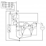
Yes indeed, though in the end I've learned a lot in a very short space of time. I have what I think is a setup free of any of the aforementioned obstacles to getting accurate results. The biggest issue by far was that the signal generator and the oscilloscope are both connected internally to mains earth ( ground )
By a process of elimination I've got interference at the amplifier input down to a level that it is beneath the noise floor of the amplifier.
See attached schematic.
Attachments
I have continued to refine my setup, it's now able to measure 10's of megohms without much difficulty. Continue to have a problem with a VLF signal superimposed on the CCS current ( the same 2 transistor 5mA CCS ) I have no idea why this is happening, but it is definitely originating in the CCS.
I have decreased the value of the coupling capacitors to reduce the gain of the amplifier at the approx 0.4Hz frequency of the problem signal. I think I'm going to have to build an additional active high pass filter with f(3db) around 10 Hz.
Elvee, did you find any evidence of this 0.4Hz signal from the same 2 transistor CCS?
Is there any chance it could be oscillating at this frequency? I know that this type of CCS can oscillate, but usually at much higher frequencies.
I have also measured the gain of the amplifier and it is within +/-0.1dB from 50 to 50 000 Hz.
Gordon.
Last edited:
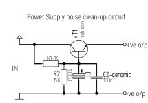
Returning to the theme of noisey voltage regulators, I found an interesting addendum to clean up noisey regulator output. See attached.
Source: Finesse Voltage Regulator Noise! |
I think that I'll give this a try. 🙂
Source: Finesse Voltage Regulator Noise! |
I think that I'll give this a try. 🙂
Attachments
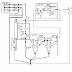
I suggest you add two pre-load resistors directly across the terminals of your dual output power supply. 1.2K@1W across C1 and 470R@1W across C2.
I also suggest you replace Rbias in the CCS subcircuit, with the four component "zero TC current source" circuit found in the LM334 datasheet and shown below. LM334 is rated for currents between 2uA to 5mA; luckily your ~500uA current thru Rbias is right in the LM334 sweet spot.
Or if you are reluctant to replace 1 resistor with 4 components, perhaps you would feel better about replacing 1 resistor with 3 components. Split Rbias into two series resistors, 20K each, and connect a 330uF bypass capacitor between the middle node of the 20K resistors, and the bottom leg of R-sense (at the intermediate star-ground).
Since the +25V supply is imperfect, it will include unwanted noise and unwanted back-injected signal (thru R-top). You want to prevent this from reaching the base of T2. The LM334 circuit does so by constructing an impedance divider with giant attenuation. The RCR circuit is merely a lowpass filter.
Attachments
Nothing of the kind, it seemed completely steadyElvee, did you find any evidence of this 0.4Hz signal from the same 2 transistor CCS?
No, only thermal oscillations are possible for these frequencies;Is there any chance it could be oscillating at this frequency?
Another possibility is a beat between hum frequency and your test frequency: 50Hz and 500.4Hz for example (or the sampling frequency of your DVM)
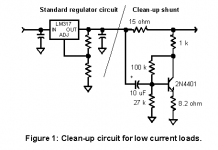
The concept could work, but not in the conditions shown: with these resistors values, that is just ordinary audiophoolery. At best, without higher order effects and neglecting the 1K(!) resistor, it could reduce the noise by a 15/8.2 factor, but in reality it will be even lower. To properly assess all the factors, it should be simmed, but do not expect too much, even if it is optimized. The transconductance of the transistor will be one of the limiting factorsReturning to the theme of noisey voltage regulators, I found an interesting addendum to clean up noisey regulator output. See attached.
I suggest you add two pre-load resistors directly across the terminals of your dual output power supply. 1.2K@1W across C1 and 470R@1W across C2.
Can you explain the advantage of adding these resistors?
I also suggest you replace Rbias in the CCS subcircuit, with the four component "zero TC current source" circuit found in the LM334 datasheet and shown below. LM334 is rated for currents between 2uA to 5mA; luckily your ~500uA current thru Rbias is right in the LM334 sweet spot.
My intention is to evaluate the relative merits of different CCS configurations and the effect that different transistors have on them.
Since the +25V supply is imperfect, it will include unwanted noise and unwanted back-injected signal (thru R-top).
I have managed to eliminate most of the back injected signal from reaching the amplifier via Rsense with a star ground scheme and care with layout, I had not considered the route via Rbias. Someone else had eluded to this earlier in the thread, speaking of the PSRR of the CCS, this is basically a special case of that in that it is test signal bleed through getting into the CCS rather than power supply hum and / or noise.
That is an important consideration, thank you for bringing it to my attention.
Gordon.
Another possibility is a beat between hum frequency and your test frequency: 50Hz and 500.4Hz for example (or the sampling frequency of your DVM)
It seems doubtful though as it persists over a wide range of test frequencies. Also it has been observed on 3 different DVM's and an oscilloscope. Can you suggest any other solution than the high pass filter?
The concept could work, but not in the conditions shown: with these resistors values, that is just ordinary audiophoolery. At best, without higher order effects and neglecting the 1K(!) resistor, it could reduce the noise by a 15/8.2 factor, but in reality it will be even lower. To properly assess all the factors, it should be simmed, but do not expect too much, even if it is optimized. The transconductance of the transistor will be one of the limiting factors
The 1K resistor seemed ludicrous to me too. He shows a better circuit further down the page if you follow the link with an lm833 and a transistor. This guy makes his living as far as I know, designing and selling ultra low noise rf amplifiers and oscillators.
Gordon.
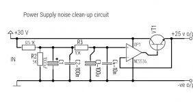
EDIT: I have attached a 40dB very low noise ( < 1nV/√Hz ) amplifier that he designed.
Attachments
Last edited:
Another idea for a low noise voltage regulator:

Source: http://blog.audioworkshop.org/ultra-low-noise-voltage-regulator-by-zetex/#.VUqKS25BvMK
Source: http://blog.audioworkshop.org/ultra-low-noise-voltage-regulator-by-zetex/#.VUqKS25BvMK
Last edited:
And here's another, this looks promising as I have all the parts other than the voltage reference:
http://www.lcaudio.com/images/Accessories/dcreg.gif
http://www.lcaudio.com/images/Accessories/dcreg.gif
Last edited:
I suggest you add two pre-load resistors directly across the terminals of your dual output power supply. 1.2K@1W across C1 and 470R@1W across C2.
Adding these resistors increases the output current drawn from the power supplies, by 20mA and 32mA respectively. This additional current flows in the supply's output transistors (BJT or MOS), increasing their transconductance. In a BJT the transconductance is proportional to current, in an MOS the transconductance is proportional to sqrt(current). In both cases, increasing the current increases the device transconductance.
Higher transconductance in the output transistors, reduces open loop output impedance, and therefore, reduces closed loop output impedance. You want an extremely low closed loop output impedance, so the back-injected signal current thru R-set, becomes a very VERY low signal voltage at the positive supply.
Adding two resistors is a cheap way to improve the performance of your power supplies.
That is a superb idea Mark. I presume this is why certain voltage regulators have a minimum load requirement?
Thanks.
Gordon.
p.s. I'm having a rest today from electronics as the last two days have been pretty intense in that respect!
Thanks.
Gordon.
p.s. I'm having a rest today from electronics as the last two days have been pretty intense in that respect!
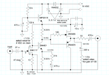
It's too late now to edit post #217, so I'll go ahead and contradict myself. Even though I said I was taking a day off from electronics, I couldn't help thinking about the attached circuit. It is intended to clean up noise from the bench PS. I'm worried though that it would increase the supplies output impedance. I think the circuits output Z is (C1||C2||R1||R2) / hFE+1, do you think that this would be higher than the direct output of the bench PSU?
Gordon.
Gordon.
Attachments
John Walton, a prolific member of diyAudio, published an informative article in Linear Audio magazine. The editor has put several of John's color figures online for free download, including (Figure 8: Output Impedance vs Frequency for several positive voltage regulators)
As you can see, his measured result for the LM317 is 2.5E-2 ohms (25 milliohms) between 10Hz and 500Hz. Other voltage regulators were considerably better; they had considerably lower output impedance.
You can compare 25 milliohms @ 100Hz, against the output impedance of your capacitance multiplier circuit. (link 1) , (link 2) , (link 3) , (link 4) . Don't forget the (1/gm) contribution to emitter follower Zout!
Last edited:
Mark thanks for your detailed reply.
Yes I forgot about the 1/gm contribution, that brings us back to your idea of load resistors to increase the value of gm and hence lower output impedance, is that right?
I tried using a 7812 to improve the source impedance and hopefully to reduce noise, it failed teribley on the latter count, output noise was 800uV peak to peak, don't think the lm317 is much better in this respect. I was thinking about maybe augmenting the capacitance multiplier with a low noise opamp, see attached.
I forgot to include the output load resistor.
Gordon.
Attachments
- Status
- Not open for further replies.
- Home
- Amplifiers
- Solid State
- How do you calculate impedance of a current source?