…
P1 value?
2K for all versions.
…
What do you think of mosfet version?
I'll skip this one. It looks like excellent results are attainable with the BJTs versions.
What's considered high impedance & low impedance for the buffers?
I don't have definite figures though it depends much on the input impedance of the power amp.
It seems to me, off hand, that < or = 200 Ohm is more than enough for 10-20K input impedance of the power amp. Lower output impedance may be beneficial for headphones amp, or maybe to drive difficult filters.
P.S.,
R1 and RL1 can be higher than 100K, I intend using 250K, though it shouldn't make much difference.
R1 and RL1 can be higher than 100K, I intend using 250K, though it shouldn't make much difference.
P.S.,
R1 and RL1 can be higher than 100K, I intend using 250K, though it shouldn't make much difference.
RL1 is R12?
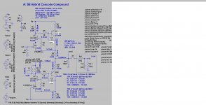
Attached schematic "D" KSA1381 mod, is OK?
Yes.
Adding the 100 Ohm resistor in series with the gates is a very good idea, to prevent possible oscillations. It's also recommended for all other versions.
You can increase R101 and R112, if you wish, or you can leave them as they are, 100K.

Hi,
regarding #561 (565):
I wouldn´t suggest making R1 (R101) higher than 100k.
It´s the input impedance the sourcing device will ´see´.
Originally I thought of AC-coupling the Buffer.
Therefore a first 100k resistor would have been added from ´in(vsine)´to gnd, and a series cap from ´in (vsine)´ to ´in(Ri)´ of 1µF to 10µF.
The first 100k and the R1 would have resulted in ~50kOhm AC-Input impedance.
The standard value for the input impedance is 47k.
So, if one wants to DC-couple the Buffer, than R1 (R101) may be reduced to 47k.
Don´t forget the Input RC lowpass Ri/Ci between ´in´ and ´in1´ (in2).
R12 (R112) are only used as ballast resistors, if no load is attached.
100k is high enough, but 250k won´t make much difference (apart from higher output offset voltage, resp. higher sensitivity to offset).
Rs, RL and CL are only external loading parts for simulation purposes!
They are no parts to be placed on the buffer PCB.
X1 (X101) are just monikers for a connecting cable.
jauu
Calvin
Thanks Calvin.
Your suggestions are noted, so I go back from my suggestion to possibly increase those 100K resistors.
Your suggestions are noted, so I go back from my suggestion to possibly increase those 100K resistors.
when you have disconnected the interconnect cable.Hi,
regarding #561 (565):
I wouldn´t suggest making R1 (R101) higher than 100k.
It´s the input impedance the sourcing device will ´see´..............
When the source is connected the input sees the source impedance in parallel to this 100k, (or 1M0 if you want to go that high).
When the input is AC coupled (i.e. has a DC blocking capacitor between Source and Receiver) the Receiver input still sees the Source impedance in parallel to that 100k. The difference is that as DC is approached the source impedance becomes higher.
Hi,
Connected to the Buffer the sourcing device will see Ri+R1 from DC to the upper bandwidth limit defined by Ri/Ci.
As Ri is small it may be neglected.
Hence from DC to a couple of hundreds of kHz the source will see 100k.
Adding the suggested first 100k and a series Cap, the source will see the first 100k from DC to a few Hz, till the Cap opens up.
From a few Hz to a few more Hz the impedance drops from 100k to 50k as the first 100k and R1 appear in parallel.
Alternatively one could reduce R1 to 47k and just add the series cap ahead.
But I like to split the input Rs this way, because it keeps DC impedance reasonably low and it bleeds off any possible charge of the cap.
If not used charge and respectively high voltages could build up and if You connect the source device 'hot' a loud thumb noise in the spekers and even destruction of devices may occur.
If used with DC free sources or as subassembly within a device, the Buffer may be DC coupled, reducing R1 to 47k, or it may even be omitted with alltogether, as it is the case with the Paradise phono stage.
jauu
Calvin
No, if not connected the source device will just see its own open output.when you have disconnected the interconnect cable.
Connected to the Buffer the sourcing device will see Ri+R1 from DC to the upper bandwidth limit defined by Ri/Ci.
As Ri is small it may be neglected.
Hence from DC to a couple of hundreds of kHz the source will see 100k.
Adding the suggested first 100k and a series Cap, the source will see the first 100k from DC to a few Hz, till the Cap opens up.
From a few Hz to a few more Hz the impedance drops from 100k to 50k as the first 100k and R1 appear in parallel.
Alternatively one could reduce R1 to 47k and just add the series cap ahead.
But I like to split the input Rs this way, because it keeps DC impedance reasonably low and it bleeds off any possible charge of the cap.
If not used charge and respectively high voltages could build up and if You connect the source device 'hot' a loud thumb noise in the spekers and even destruction of devices may occur.
If used with DC free sources or as subassembly within a device, the Buffer may be DC coupled, reducing R1 to 47k, or it may even be omitted with alltogether, as it is the case with the Paradise phono stage.
jauu
Calvin
the input to the Buffer is connected to a Source AND to the Rin setting resistor.Hi,
No, if not connected the source device will just see its own open output...........
As far as the Buffer is concerned, the Buffer sees the Rin in parallel to the Source's output impedance.
If one disconnects the interconnect, then the Buffer sees the Rin alone.
Hi,
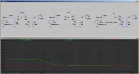
shown are the three possibilities for the input filters.
red: as is in the simu of #561
blue: as is plus AC-coupling cap
green: with split Rs and AC-coupling cap
The input impedance plots as the source would see them(1st attachment).
red: 50k (50k390 to be precise) until the Ci comes to effect lowering the curve above 10kHz.
blue: as red, but rising to infinite (an open) below 1Hz
green: as blue but Rin limiting the plot to 100k below ~100mHz.
Over the range of ~1Hz to 10kHz the source mostly sees Rin and R1 in parallel (50k).
If a source with miniscule output impedance is connected the JFETs will see impedances as shown in the 2nd attachment.
red: constant at 390R (value of Ri, Ci has nearly no effect below 100kHz)
blue: like red at 390R, but rising below ~10Hz and levelling out at 50kOhm below~100mHz.
green: similar to blue but levelling out at 100kOhm below ~100mHz.
Of importance is rather what the impedance seen from the source looks like (1st attachment).
jauu
Calvin
Attachments

Of importance is rather what the impedance seen from the Buffer looks like when looking back towards the Source
Only when the interconnect is disconnected does the Buffer see Rin alone.
If one also has an RF attenuating capacitor (as shown in your sch) then the disconnected impedance seen by the Buffer is Cin||Rin. i.e. even lower and at RF extremely low.
Only when the interconnect is disconnected does the Buffer see Rin alone.
If one also has an RF attenuating capacitor (as shown in your sch) then the disconnected impedance seen by the Buffer is Cin||Rin. i.e. even lower and at RF extremely low.
Last edited:
Hi,
Yes, the Ci shunts RF away from the JFET's Gate.
The Gate is grounded at RF.
So that's perfect, as we want no RF entering the Buffer.
At the same a connected source would still see the 390R as load at RF.
That might be a bit low as load for OPAmp chips, but nothing destructive and certainly better than a dead short.
jauu
Calvin
- Home
- Source & Line
- Analog Line Level
- Preamp-Buffers - simple idea