The CRC snubber at work
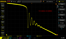
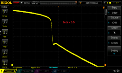
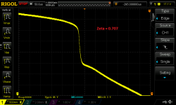
Just for illustration, I'm attaching waveforms for different values of Zeta, measured in a working power supply. Referring to the Excel table in post #486, it is the entry in row 11, i.e. a simple wall plug, 12V/500mA power supply, loaded for the measurement with a 330R resistor (approx. 50mA).
The snubber configuration used is Cx=10nF, Cs=150nF, Rs,max=1K.
The first plot shows the waveform at the transformer secondary with Cx in place, but without snubber; it rings, as expected.
The following three plots refer to the Zeta values of 0.5 (Rs=487R), 0.707 (Rs=340R), and 1 (Rs=239R), respectively. At Zeta=0.5, the secondary is not yet quite damped, whereas the waveforms at Zeta=0.707 and 1.0 indicate a properly damped behaviour, and are almost indistinguishable from each other. This speaks in favour of choosing Zeta=1 as the criterion for determining the snubber resistance, since it trades a negligibly higher loss for robustness in the snubber design.
Regards,
Braca
Attachments

If anyone intends to fool around with CRC snubbers at zeta>1.0 (outside the recommended range of "Simple no-math transformer snubbers"), I strongly suggest you slog your way through the Laplace domain math that includes all three of Cx, Rs, Cs. Sorry, the no-math approach includes a few simplifications and one of these is that zeta is around 1.0. Hagerman's snubber paper shows one possible approach to writing out the appropriate equations.
I predict that after a few pages of algebra, you'll conclude that oscillations do not remain damped unless (Cs >= (15 * Cx * zeta)). For "no-math snubbers" having zeta=1, this simplifies to (Cs >= (15 * Cx)) and indeed the Quasimodo starting recommendation is Cs=150nF and Cx=10nF ... a factor of exactly fifteen.
However, if for some inexplicable reason you wish to explore zeta >= 10, you won't get the overdamped non-oscillations you expect unless you set (Cs >= 150 * Cx). Depending on your own personal inventory of low dissipation factor (tan δ) film capacitors in your parts box, that might be {Cx=10nF, Cs=1.5uF} or, more likely, {Cx=2.2nF, Cs=330nF}.
Last edited:
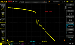
could you generate the Zeta = 10 plot and post?
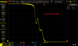
Andrew, even without performing a measurement at Zeta = 10, the response of the circuit can easily be predicted. Since the Hagerman's theory produces Rs=23R in this case, which effectively leads to Cs being connected parallel to Cx, the system will oscillate at the natural frequency defined by (Lt, Cx+Cs). In this particular case, this frequency is approx. 8550Hz. The ringing will be damped by the sum of the secondary winding resistance and Rs, and by whatever other dissipation mechanisms that may be present.
For the fun of it, I'm enclosing an oscillogram of this configuration. The period of the single oscillation visible is roughly the half of the 200us time base interval, which comes close to the above mentioned value of 8550Hz.
So the response is not damped, as Mark rightly points out, because it is not the same system any more, i.e. the one composed of (Lt, Cx).
Regards,
Braca
Attachments
DnI, why not run your test with Rs=23R, Cx=10nF, Cs=1500nF? This will show what a severely overdamped (zeta=10) waveform actually looks like. {any Cs >= 1.5uF will be equally good}
The label in your post #504 photo might be a little misleading; the experiment is not really "zeta=10" , but rather "Rs=23".
The label in your post #504 photo might be a little misleading; the experiment is not really "zeta=10" , but rather "Rs=23".
Last edited:
That confirms what I found with my cheapo.Andrew, even without performing a measurement at Zeta = 10, the response of the circuit can easily be predicted. Since the Hagerman's theory produces Rs=23R in this case, which effectively leads to Cs being connected parallel to Cx, the system will oscillate at the natural frequency defined by (Lt, Cx+Cs). In this particular case, this frequency is approx. 8550Hz. The ringing will be damped by the sum of the secondary winding resistance and Rs, and by whatever other dissipation mechanisms that may be present.
For the fun of it, I'm enclosing an oscillogram of this configuration. The period of the single oscillation visible is roughly the half of the 200us time base interval, which comes close to the above mentioned value of 8550Hz.
So the response is not damped, as Mark rightly points out, because it is not the same system any more, i.e. the one composed of (Lt, Cx).
Regards,
Braca
Too little resistance gives oscillation.
Too much resistance gives oscillation.
The damping resistor must be in an acceptable range.
DNI, why don't your charts look like the standard charts which are symmetric about the X-axis?
BigE, they only show the details of the ringing phenomenon (note the 500mV vertical resolution). Had I shown the complete picture (an 18 Volt pulsation from a 12V PS), the ringing part of the curve would have been scarcely visible.
So do mine, yet they are vastly different.
Maybe it is because of the power ? I'm using a 9 volt battery for power.
Maybe it is because of the power ? I'm using a 9 volt battery for power.
So do mine, yet they are vastly different.
Maybe it is because of the power ? I'm using a 9 volt battery for power.
Please note that they do not represent waveforms obtained by Quasimodo, but the ones measured at a filter capacitor in a working power supply.
The idea was to show the effects of the snubber in application.
DnI, why not run your test with Rs=23R, Cx=10nF, Cs=1500nF? This will show what a severely overdamped (zeta=10) waveform actually looks like. {any Cs >= 1.5uF will be equally good}
The label in your post #504 photo might be a little misleading; the experiment is not really "zeta=10" , but rather "Rs=23".
Apologies first: Due to a typo, the secondary winding resistance of the transformer used for the current discussion is 18 ohm instead of the correct value of 1.8 ohm. The error has almost no effect at low damping values, but 18 ohm is a lot of damping in the "Zeta=10" case. I'm enclosing a corrected version of my Excel spreadsheet. Please discard the previous version.
Re. the above label on my plot: There is nothing in the theory that forbids setting Zeta=10 as long as the circuit structure remains the same. Since, however, at Rs=23R the circuit structure is a tank with (Lt,Cx+Cs), i.e. not any more the one with (Lt,Cx), Rs=23R with Cs=1.62uF I used for the measurement. So my labeling the plot with Zeta=10 is misleading.
The above damping factor value, i.e. 0.375, entered temporarily into cell G3 of the spreadsheet along with Cx=1.62E-6 in cell C3 results in Rs=22.7R in cell J11. Please dont't forget to restore the original values in cells C3 and G3 after finishing this exercise!
A measurement with Rs=23R and Cs=1.62uF does indeed produce an undamped waveform that is to be expected from these values. Results similar to the measured one are also obtained from the LTspice simualtions of the Cheapomodo and the power supply I used for the measurement.
In conclusion, there is no reason to go for high Zeta values when designing the snubber. Zeta of about unity provides ample damping of the parasitic oscillations at rectifier diode's switching off without the risk of waking up the sleeping dog at (Lt,Cx+Cs).
Regards
Attachments
Another apology:
The 2nd paragraph of my above post is incomplete. It should have read:
Re. the above label on my plot: There is nothing in the theory that forbids setting Zeta=10 as long as the circuit structure remains the same. Since, however, at Rs=23R the circuit structure is a tank with (Lt,Cx+Cs), i.e. not any more the one with (Lt,Cx), Rs=23R with Cs=1.62uF I used for the measurement result in a damping factor of 0.375 at the new natural frequency of 2663Hz. So my labeling the plot with Zeta=10 is misleading.
Regards
Last edited:
In the documentation, it is suggested that the snubber be installed as close to the transformer as possible. Would there be any significant difference if it was installed on top of the diode bridge instead? I have the possibly mistaken idea that the snubber is eating the diode noise, if so then the closer to the diodes the better.
As I read it every mains pulse ´rings a bell´. The bell is the transformer, so the snubber is dampening the transformer ringing.
Hope I am right.
Best regards
Arthur.
Hope I am right.
Best regards
Arthur.
the transformer secondary is connected to the bridge rectifier.In the documentation, it is suggested that the snubber be installed as close to the transformer as possible. Would there be any significant difference if it was installed on top of the diode bridge instead? I have the possibly mistaken idea that the snubber is eating the diode noise, if so then the closer to the diodes the better.
There is no closer place than the bridge rectifier to the transformer secondaries.
Mount the rectifier direct to the secondary.
Mount the snubber across the rectifier.
In the documentation, it is suggested that the snubber be installed as close to the transformer as possible. Would there be any significant difference if it was installed on top of the diode bridge instead? I have the possibly mistaken idea that the snubber is eating the diode noise, if so then the closer to the diodes the better.
The documentation is the best recommendation. In practise, the earliest opportunity to connect to a secondary winding may be at the rectifier bridge/diode where the transformer wires are terminated.
the transformer secondary is connected to the bridge rectifier.
There is no closer place than the bridge rectifier to the transformer secondaries.
Mount the rectifier direct to the secondary.
Mount the snubber across the rectifier.
In my case, there is a closer place, since I've inserted a barrier strip to convert the paralleled secondaries to a single wire per channel.
The snubbers are being mounted there.
Have you achieved low loop area AND compact layout, when you added extra wiring and the barrier strip?In my case, there is a closer place, since I've inserted a barrier strip to convert the paralleled secondaries to a single wire per channel.
The snubbers are being mounted there.
The wiring from the transformer has been cut quite short. From there, the wiring needs to have the CT lines ( one per channel ) moved to be nearer the secondaries to decrease loop area.
There will be areas where the CT line cannot make zero loop area with the secondaries. eg. rectifiers and relays.
Right now, the error is that the CT line goes straight to the capacitor bank and is quite independent of the path of the secondaries.
There will be areas where the CT line cannot make zero loop area with the secondaries. eg. rectifiers and relays.
Right now, the error is that the CT line goes straight to the capacitor bank and is quite independent of the path of the secondaries.
twist the CT wire with the two secondary wires.
Take this twisted triplet to the rectifier.
Pass the CT wire straight across the rectifier.
Connect the two secondary wires to the rectifier.
Twist the CT wire with the two DC wires from the rectifier.
Take the twisted triplet to the smoothing capacitors.
Terminate the three wires on the first stage smoothing caps.
Keep the LOOPS at each end of the twisted triplets as small as possible.
This minimises loop area AND uses cancellation of fields in each wire to attenuate the emitted radiation even lower than close coupled triplet.
- Home
- Amplifiers
- Power Supplies
- Simple, no-math transformer snubber using Quasimodo test-jig