Is it possible to post as PDF?... just sent to fab.
As always schematics and pcb gerber files are free to use only for non commercial DIY projects.
Have fun,
Toni
Is it possible to post as PDF?
Gerber files can be read/printed using e.g.:
Windows: GC-Prevue
Linux: gerbv
Attached PDF's for those who want to print pcb layout directly.
Have fun,
Toni
Attachments
Dear Andrew,Astx,
well done, a very thorough design exercise.
I hope it sounds good.
many thanks to you and all others who have contributed to this thread and have helped finetuning this amplifier.
Many thanks goes to Bob Cordell and Douglas Self too!
IMHO: it sounds very good (of course only mono testing has been done so far). The "big" test has to wait till end of july ...
BR, Toni
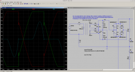
One step forward eliminating the need of a M$ operating system: Today I got ARTA running under openSUSE 13.1 using wine 1.7.17 (setup doesn't work under wine, but copying the installed files from windows / "Program Files (x86)/ArtaSoftware" to linux wine drive_c works)
Attached ARTA device settings under Linux using Asus Xonar STX. You can control the device settings using the console program "alsamixer". Switching output to headphone or line out, control headphone impedance ...
Awesome!
See attached pictures of some settings and a redone IMD measurement as I was now able to use the headphone outputs instead of line out.
Pictures:
- ARTA devices settings under linux/wine
- alsamixer settings
- IMD reference of soundcard
- IMD 50W@8R
- IMD 100W@8R
- IMD 200W@8R
For me setup works perfectly under wine-1.7.15
Measurement software
Running wine 1.7.2 and ArtaSetup182.exe is also OK but not using wine 1.7.17
Thx for info. Which setup version of ARTA have you installed?For me setup works perfectly under wine-1.7.15
Running wine 1.7.2 and ArtaSetup182.exe is also OK but not using wine 1.7.17
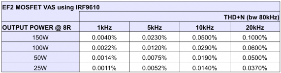
[*]The factor is even worse. More as 100 times higher THD at full power 20kHz real life versus simulation. The sentence "THD isn't so far away from simulation." was meant as a joke! 😉
Hi Toni
I just had a closer look at this.
You seem to have used the LTSpice level 3 monolithic model for your MOSFET simulation.
This is not a suitable model for distortion simulation, no matter what values you use, it doesn't model variable capacitance properly.
The rest of the work looks nice, my compliments.
Best wishes
David
...
You seem to have used the LTSpice level 3 monolithic model for your MOSFET simulation.
...
Dear Dave,
thanks! What would you like to drink?

Is there a better MOSFET model we can use in LTSpice or do we currently have no chance to do meaningful MOSFET distortion analysis in simulation?

Is there a better MOSFET model we can use in LTSpice or do we currently have no chance to do meaningful MOSFET distortion analysis in simulation?
There is some information buried away in the LTSpice help but Cordell's book has the best explanation about this.
In summary, the best choice seems to be a combination of the LTSpice VDMOS and EKV models.
This handles both variable capacitance and sub-threshold conduction.
You will practically never find a manufacturer who provides models in this format so you will have to extract all the model parameters yourself.
Your practical results and Samuel's comments have not provided much incentive to explore this and I haven't looked at it much myself.
I am a bad Australian, I like lambic beers from Amsterdam....What would you like to drink?
I hope to be in the Tyrol next summer, perhaps we can share one😉
Best wishes
David
Last edited:
A very good hint: found VDMOS models from andy_c here...
In summary, the best choice seems to be a combination of the LTSpice VDMOS and EKV models.
...
FQP2P25 as replacement for IRF9610 using this model gives nearly exactly the same (bad) THD results as my real life measurements
THD20k: 0.06% @ 50W @ 8R.
(right picture: real life measurements using VP7723-D)
This would be very nice if we could meet us testing different sorts of austrian and german beers...😉...
I am a bad Australian, I like lambic beers from Amsterdam.
I hope to be in the Tyrol next summer, perhaps we can share one😉
...
Attachments

Last edited:
A very good hint: found VDMOS models from andy_c here
FQP2P25 as replacement for IRF9610 using this model gives nearly exactly the same (bad) THD results as my real life measurements
THD20k: 0.06% @ 50W @ 8R.
(right picture: real life measurements using VP7723-D)
Thanks alot! I had not found these myself yet.
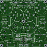
SA2013 V3.4 power supply
Schematics and pcb gerber files are free to use only for non commercial DIY projects.
WARNING: this circuit provides very high DC voltages and is therefore very dangerous and can be lethal. I am not responsible for any costs, damage and/or injury using these schematics. Do not use this schematics if you do not have the necessary experience and knowledge.
Have fun,
Toni
Attachments
...found VDMOS models from andy_c here
...this model gives nearly exactly the same (bad) THD results as my real life measurements...
Nice that my recommendation was useful and led to further discovery.
I had not seen Andy's post before but it is excellent, and not just because it confirms what I said.😉
The fact that your VDMOS simulation is a close match to reality without the extra complication of the EKV model is useful too.
Best wishes
David
Hi Toni,
I do not see any R-C snubbers in the PS design, thought to offer a suggestion to use the Quisomodo to determine the correct snubber network for the transformer you have chosen, as an small improvement.
I bought the small pcb/parts (from user "dsolodov") and have been playing with it. It works very well. Hope it helps, if you are interested.
http://www.diyaudio.com/forums/powe...sformer-snubber-using-quasimodo-test-jig.html
See post #345
Cheers
Rick
...
I do not see any R-C snubbers in the PS design, thought to offer a suggestion to use the Quisomodo to determine the correct snubber network for the transformer you have chosen, as an small improvement.
...
Cheers
Rick
Dear Rick,
thank you for hint. Will have a deeper look at this.
BR, Toni
And following the quasi modo hint,
remove capacitors C1, 2, 3, 4, 5, 6, 7, 8, 19 & 30
Move snubber C17+R7 to Tx terminals 3 & 4
Move snubber C18+R8 to Tx terminals 1 & 2.
Adjust snubber values to suit the transformer.
remove capacitors C1, 2, 3, 4, 5, 6, 7, 8, 19 & 30
Move snubber C17+R7 to Tx terminals 3 & 4
Move snubber C18+R8 to Tx terminals 1 & 2.
Adjust snubber values to suit the transformer.
And following the quasi modo hint,
remove capacitors C1, 2, 3, 4, 5, 6, 7, 8, 19 & 30
Move snubber C17+R7 to Tx terminals 3 & 4
Move snubber C18+R8 to Tx terminals 1 & 2.
Adjust snubber values to suit the transformer.
IMHO: removing all this capacitors would be the same as to concentrate only on one problem - transformer resonance due to rectifier switching.
For an updated power supply version I would do following changes:
- add second rectifier bridge to isolate the 2 secondaries to avoid DC current flowing through transformers.
- add CRC snubbers to each secondary.
Attachments
I have been following this rather remarkable project for a couple of weeks now. Congratulations on a fantastically performing amp with a truly professional build!
I'm very new to all this and learning a lot. This part of the conversation will be particularly interesting as I've spent more time on power supplies so far.
(Having used the Quasimodo I must admit I was thinking the same as Andrew regarding removing the caps across the rectifier diodes and I think you guys are more or less saying the same thing with respect to the snubbers. Agree also re the other bridge.)
Can I ask a very basic couple of questions:
- what heatsink are you using for the diodes (I could not find similar on Mouser) and where do you source your Cooltec enclosure heatsinks?
- what's the purpose of the holes in the PCB around the centre mount hole and between the two heatsinks?
- I assume the vias under the caps are to link the ground planes; what's the purposes of the 3 solid connections rather than traces - two between C3 and C4 and one to the right of the heatsink?
Forgive me if these are too basic!
Regards
Steve
THX! 😉I have been following this rather remarkable project for a couple of weeks now. Congratulations on a fantastically performing amp with a truly professional build!
- what heatsink are you using for the diodes (I could not find similar on Mouser) and where do you source your Cooltec enclosure heatsinks?
- what's the purpose of the holes in the PCB around the centre mount hole and between the two heatsinks?
- I assume the vias under the caps are to link the ground planes; what's the purposes of the 3 solid connections rather than traces - two between C3 and C4 and one to the right of the heatsink?
- Cooltec heatsinks I have bought directly. Visit their homepage at www.cooltec.de
- Diodes heatsink: used Fischer Electronics SK76 / 75mm (input/VAS stage uses SK76 / 25mm)
- holes in centre is for better cooling the big electrolytics.
- holes under SK76 is for better cooling too.
- the pcb (70µm copper) is designed to be 1-sided so you need 3 solid wires. To get better autorouting I have run the pcb program 2-sided. So the pdf may include too much information. From top layer use only the silk screen.
Toni
- Home
- Amplifiers
- Solid State
- 2stageEF high performance class AB power amp / 200W8R / 400W4R