.... and mind reader, too ?? 🙂
Maybe we can get insights in this aspect from Bob C. and his FET OPS designs. I have used some of them specifically for their neg thermal coeff and other benefits but lets hear from The Man as he is a strong proponent.
OOOooooH, BOB !! Can you come over here for a minute ??
THx-RNMarsh
Hi Richard,
Good point. MOSFETs, be they Lateral or Vertical, are much better in the thermal stability department, and usually cannot be biased into gm doubling because of their limited transconductance. Note that it is also difficult if not impossible to bias a tube amp into gm doubling.
Laterals are indeed more thermally stable than Verticals because they do transition to a negative TC in a current range not that different from where they are usually biased. Moreover, since they don't have gm doubling, and because they need to in order to get higher gm to reduce their transconductance droop caused crossover distortion (kind of like the inverse of gm doubling, but much softer), MOSFETs are usually biased higher than BJTs, so they may naturally keep the amplifier a bit more toasty. Also, partly because of this, it takes a much bigger thermal swing on program dynamics to get them into a seriously under-biased condition.
Verticals are a step closer to BJTs as compared to Laterals, but they are still far superior to BJTs in the thermal stability department. Verticals do eventually get to a negative TC, but it occurs at a much higher current, in the Amperes. While Laterals can get away with no Vbe multiplier that is attached in some way to the heat sink, properly designed vertical mosfet power amps do need some degree of modest
thermal feedback compensation.
Take a look at the thermal stability curves I presented in my old MOSFET EC paper.
The advent of ThermalTrak BJTs, in my opinion, has largely rescued the BJT technology from much of the thermal stability problems. I have shown this with thermal stability curves in my book for BJT amplifiers with and without ThermalTrak diodes engaged.
MOSFET amplifiers are an example of amplifiers that have higher static distortion on the bench, but often sound better.
Cheers,
Bob
Too complex Dave. Keep it simple
Yes, I like simple too.
But this is no more parts, just a little tweak.
And I known audiophiles LOVE to tweak their equipment, expected someone's tried this.
Other people must have looked at Self's plots of the effect of bias current and noticed that if you offset them then the bumps of one partly cancel the dips of another, same as the multi-tan IPS.
Except with no extra transistors.
And helps the OPS, where most of the distortion is, rather than the IPS, which hardly needs it.
Just reminded of the idea with all the talk of the benefits of lower Re.
Now you can have both! And it's new and unique.
And even makes some sense, unlike a lot of amplifier ideas😉
Best wishes
David
Last edited:
Hmmm. how well one can keep the BJT OPS bias always locked on the thd null point will be an important design parameter. I havent appreciated this enough before.
I see now there has been quite a lot of work in this area. However, not much has filtered down to a lot of the makes and models, it seems. I dont have my reference books avail to me at this time... but I did read Bonsai's paper on the dual-point thermal compensation and am wondering if there is a easy way to add a part or two to the stock 1-2 transistor bias spreader circuit which will change it to more like a dual point comp bias circuit... quasi? Any suggested circuits/mods ideas for DIY'er?
THx-RNMarsh
to the question of the emitter (of source) resistors in the output stage (OPS) of the amplifier: Technical Brain TBP-Zero EX Amp & TBC-Zero EX Preamp (TAS 213) | The Absolute Sound
best regards
Petr
best regards
Petr
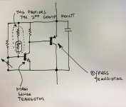
Here is how to do it with a resitor and an NTC.
The main sense transistor provides the ambient cal point, and the NTC the second cal point.
In the article you read Richard, I looked at using a low power op-amp, and in a derivation of that circuit, a TL431LV.
The technique below works just as well and is simpler.
The main sense transistor provides the ambient cal point, and the NTC the second cal point.
In the article you read Richard, I looked at using a low power op-amp, and in a derivation of that circuit, a TL431LV.
The technique below works just as well and is simpler.
Attachments
Last edited:
Andrew, presumably this is what's described in your #6290 post.Here is how to do it with a resitor and an NTC.
The main sense transistor provides the ambient cal point, and the NTC the second cal point.
It looks elegantly simple .. which is of course, the highest praise I can give. 🙂
But what is in Thermal Contact with what?
Are both the NTC & "MAIN SENSE TRANSISTOR" on the Heatsink? What about "BYPASS TRANSISTOR" ?
No complaints ...
With the 2 device EF3 Vbe i'm using ....
sub mV bias errors in the REAL world.
T-track might be better , but us "poor people" with our E-waste sankens
have to make due with the best we can design. 😱😱
OS
With the 2 device EF3 Vbe i'm using ....
sub mV bias errors in the REAL world.
T-track might be better , but us "poor people" with our E-waste sankens
have to make due with the best we can design. 😱😱
OS
Richard,
The sense transistor is located next to the emitter lead of one of the output transistors. I use a BC847C.
The NTD is located next to the emitter lead of one of the other output transistors - coupled with a small amount of thermal grease.
The pass transistor is a free standing TO-126 (I could actually have used a TO-92 - but I used a TO-126).
The idea of two point (or multiple point) thermal comp is to make the thermal comp curve as flat as possible so it tracks the ideal bias temperature more accruately. This way the delta between the actual bias current and the ideal bias current is smaller and the system then get to equilibrium more quickly. Most single point thermal comp schemes look for a best fit and use a single cal point.
Note that we are taking a classic bias spreader and just helping it to perform a bit better by calibrating it so it intersects the ideal bias current in two places by design. Good thermal design then completes the job.
OS if its any consolation, I also don't use T-track either, although with 2 point comp, I think you could really make it sing.
Re the MCU thermal comp approach, I would just put it directly across the bias spreader - no need to opto coupling. These new low power MCU's are also nice and quiet because you can turn off all the peripherals you dont need and run them with a slow clock.
(Go with the LPC 😉
(Go with the LPC 😉
Thanks for this Andrew.The sense transistor is located next to the emitter lead of one of the output transistors. I use a BC847C.
The NTD is located next to the emitter lead of one of the other output transistors - coupled with a small amount of thermal grease.
The pass transistor is a free standing TO-126 (I could actually have used a TO-92 - but I used a TO-126).
The idea of two point (or multiple point) thermal comp is to make the thermal comp curve as flat as possible so it tracks the ideal bias temperature more accruately. This way the delta between the actual bias current and the ideal bias current is smaller and the system then get to equilibrium more quickly. Most single point thermal comp schemes look for a best fit and use a single cal point.
Note that we are taking a classic bias spreader and just helping it to perform a bit better by calibrating it so it intersects the ideal bias current in two places by design. Good thermal design then completes the job.
In da 80's, I did this type of thing with a Spreadsheet. The spur was finding that CFP o/ps had really critical bias leading to nasty xover immediately after a burst of power.
When Self's book appeared, I revisited the subject but by then it was mainly academic as we were no longer making commercial amps.
I think Self's is a better treatement of 'Thermal Design' though Cordell is better for Thermal Gain. Self also favours some schemes which are wonky if the amp is cooked for a bit.
It's possible to design simple single transistor bias for EF2 with sorta '2 point' Thermal Comp by twiddling Thermal Gain but your method is a clever & useful addition to our toolbag.
And I like tools that are proven to work 🙂
___________________
But my $0.02 is that if you are using an MCU method, it better remove the need for tweaking Iq on Factory Test.
It's not sufficient to just look at the current in the emitter resistors. The MCU needs to distinguish between 'signal' current and Iq.
Thank you, good observations, and good information.Richard,
The sense transistor is located next to the emitter lead of one of the output transistors. I use a BC847C.
The NTD is located next to the emitter lead of one of the other output transistors - coupled with a small amount of thermal grease.
The pass transistor is a free standing TO-126 (I could actually have used a TO-92 - but I used a TO-126).
The idea of two point (or multiple point) thermal comp is to make the thermal comp curve as flat as possible so it tracks the ideal bias temperature more accruately. This way the delta between the actual bias current and the ideal bias current is smaller and the system then get to equilibrium more quickly. Most single point thermal comp schemes look for a best fit and use a single cal point.
Note that we are taking a classic bias spreader and just helping it to perform a bit better by calibrating it so it intersects the ideal bias current in two places by design. Good thermal design then completes the job.
You state thermally coupling to emitter leads.
Emitter leads are thermally coupled to the die via emitter lead wire and encapsulation.
In my experience/understanding for power output transistors, the transistor die is directly mounted to the collector heatsink connection/substrate, and therefore provides the lowest thermal impedance/fastest thermal connection to the actual transistor die.
Is there a particular reason that you specify thermal connection to the emitter lead/leads ?.
Dan.
LOL......it happens to the best of us. 😉.SORRY I MEANT COLLECTOR LEAD
Had a busy week - I must be going nuts.
Dan.
Richard, with the MCU method, you would be using feed forward. No chance to measure the dynamic signal current accurately. And if you use a conventional spreader to do the first order stuff, the MCU load and required accuracy are greatly lessened.
You could characterize the first few production amps and then use that data in full production. I think the alternative is to let the MCU self calibrate during final test.
No tweaking.
(I used to design industrial instrumentation in my younger days - I know you need to avoid production floor tweaking!)
Last edited:
Member
Joined 2009
Paid Member
Richard I'm getting old too. Most of the time my right ear is full of fluid partly because of the meds I'm on but I can still tell and I think you can tell too.
A year ago or so PMA put up some wav files. One with 0.1% THD @ 1kHz, 2nd H I believe. Another with 0.01% and yet another with 0.001%. I listed to all three on crappy computer speakers with a nothing special sound card. The I took one of the files and ran it through a digital low pass filter repeatedly until the software reported 0.000000% distortion. On that file I could hear the difference. I can here the absence of distortion but if there is some I can't tell you how much it is.
A year ago or so PMA put up some wav files. One with 0.1% THD @ 1kHz, 2nd H I believe. Another with 0.01% and yet another with 0.001%. I listed to all three on crappy computer speakers with a nothing special sound card. The I took one of the files and ran it through a digital low pass filter repeatedly until the software reported 0.000000% distortion. On that file I could hear the difference. I can here the absence of distortion but if there is some I can't tell you how much it is.
- Home
- Amplifiers
- Solid State
- CFA Topology Audio Amplifiers