Hello again Edmond,
The addition of R12 & C1 (400R & 50pF) reduces the near clipping overshoot into 100nF (no parallel R) to just 5%, with no reported THD20 increase, so this is definitely worth padding out for - thanks once again.
Cheers, Ian (off to pub to watch football)!
The addition of R12 & C1 (400R & 50pF) reduces the near clipping overshoot into 100nF (no parallel R) to just 5%, with no reported THD20 increase, so this is definitely worth padding out for - thanks once again.
Cheers, Ian (off to pub to watch football)!
To all,
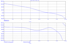
Below you see the phase and magnitude plots of the global FB loop of two nearly identical amplifiers, which differ only in the way of compensation. All other things are equal. Apart from THD, which of the two do you prefer (and why), A (1st pic) or B (2nd pic) ?
Cheers,
E.
Has that ugly freq peak at 100 and smthing anything to do with the frequency compensation method?
I've just been reading Bob's book, and noticed Fig 11.17 which uses IITMC fed from an output pre-driver! Looks like IITMC might work. Bob quotes simulation results. I wonder if he or anyone else has built it.
Hi Ihan,
I am indeed a fan of TMC, and at the same time I have always liked input compensation, from the time I first used it in my MOSFET power amplifier with error correction. Notice also that the IPS-VAS of this design is nearly the same as the one I used in the MOSFET amplifier with error correction. I did not build the amplifier of Fig. 11.17, but did quite a few simulations on it. Most schemes that leave an intermediate high-Z node want to have some series R-C compensation shunting that node to ground to establish a known and appropriate high-frequency load on that node. A scheme like ITMC helps make static distortion performance of a MOSFET amplifier competitive with BJT amplifiers while preserving the MOSFET benefits.
Cheers,
Bob
What Douglas self calls input inclusive compensation is actually phase lead compensation taken from the output of the second stage.
Hi Mike,
I used it and called it Miller input compensation long before Doug re-named it. I first used it in 1983 in my MOSFET power amplifier with error correction. As usual, Doug was a bit referencing-challenged here. Although it may look a bit like lead compensation, it was never thought of, or designed to be, lead compensation by me. The loop formed by the compensating capacitor is simply an integrator that happens to include the input stage within the amplification that forms the integrator.
Cheers,
Bob
To all,
Below you see the phase and magnitude plots of the global FB loop of two nearly identical amplifiers, which differ only in the way of compensation. All other things are equal. Apart from THD, which of the two do you prefer (and why), A (1st pic) or B (2nd pic) ?
Cheers,
E.
Hi Edmond,
The first looks like TPC, as per the plot I show in my Figure 9.5. I was able to tame it with what I called Bridged T compensation (BTC), wherein a small capacitance is shunted from input to output of the T circuit, as shown dotted in Figure 9.4. I have not seen a reference to BTC, but I would not be the least bit surprized if someone implemented it before I did. I just love this alphabet soup 🙂.
Cheers,
Bob
Has that ugly freq peak at 100 and smthing anything to do with the frequency compensation method?
Yes, it does.
edit: Also notice the phase response between 100Hz and 10kHz.

Cheers,
E.
Last edited:
Yes, it does.
Cheers,
E.
Thanks. If you don't mind, can you expand on this? I am having troubles understanding how a high frequency compensation method has such a collateral effect at 100Hz.
Yes, it does.
Cheers,
E.
Sorry, I just read Bob Cordell's replies, and now I am really confused. If the first is TPC (two pole compensation, as described by Self, I suppose) is there a LF (100 Hz or smthing) peak always associated with TPC? Trying to learn something here...
Sorry, I just read Bob Cordell's replies, and now I am really confused. If the first is TPC (two pole compensation, as described by Self, I suppose) is there a LF (100 Hz or smthing) peak always associated with TPC? Trying to learn something here...
No. The position of the poles and how damped (or not) they are depends on the circuit configuration. My paper shows a simulation of an amp with a VAS with no cascode, and the poles of the loop gain are well damped (no peaking in the loop gain).
Edmond, I'm a bit confused by the phase plot for the TPC config. I don't think the loop gain has 180 degree of phase shift at low frequency. Presumably we need to subtract 180 from the figures shown?
Hi Ihan,
I am indeed a fan of TMC, and at the same time I have always liked input compensation, from the time I first used it in my MOSFET power amplifier with error correction. Notice also that the IPS-VAS of this design is nearly the same as the one I used in the MOSFET amplifier with error correction. I did not build the amplifier of Fig. 11.17, but did quite a few simulations on it. Most schemes that leave an intermediate high-Z node want to have some series R-C compensation shunting that node to ground to establish a known and appropriate high-frequency load on that node. A scheme like ITMC helps make static distortion performance of a MOSFET amplifier competitive with BJT amplifiers while preserving the MOSFET benefits.
Cheers,
Bob
Hi Bob,
Thanks for the advice and explanation.
Cheers,
Ian
TTPC vs ETMC
Hi Bob, Harry & YWN,
Referring to post 3198, the first (left) plot is not from a TPC configuration, rather TTPC. I also was confused and amazed by the weird phase response. It's not just a matter of a wrong sign, instead, this anomaly is what you get if the circuit (actually the matrix) is near singular.
When I add a 'BTC cap = 2.2pF' (courtesy of Bob!) the phase response becomes 'normal', that is, what we would expect from a TPC configuration. Even a 1pF cap cures the anomaly.
BTW1, the second plot is from a ETMC config. and THD20=0.5ppm, while THD20 for the TTPC version is 2.5ppm.
BTW2, Bob, do you think it's possible to get rid of that ugly phase dip (and overshoot), by inserting an all-pass filter into the global NFB network?
Cheers,
E.
Hi Edmond,
The first looks like TPC, as per the plot I show in my Figure 9.5. I was able to tame it with what I called Bridged T compensation (BTC), wherein a small capacitance is shunted from input to output of the T circuit, as shown dotted in Figure 9.4. I have not seen a reference to BTC, but I would not be the least bit surprized if someone implemented it before I did. I just love this alphabet soup 🙂.
Cheers,
Bob
Hi Bob, Harry & YWN,
Referring to post 3198, the first (left) plot is not from a TPC configuration, rather TTPC. I also was confused and amazed by the weird phase response. It's not just a matter of a wrong sign, instead, this anomaly is what you get if the circuit (actually the matrix) is near singular.
When I add a 'BTC cap = 2.2pF' (courtesy of Bob!) the phase response becomes 'normal', that is, what we would expect from a TPC configuration. Even a 1pF cap cures the anomaly.
BTW1, the second plot is from a ETMC config. and THD20=0.5ppm, while THD20 for the TTPC version is 2.5ppm.
BTW2, Bob, do you think it's possible to get rid of that ugly phase dip (and overshoot), by inserting an all-pass filter into the global NFB network?
Cheers,
E.
Attachments
post3198.
Please explain how to read the two sets of plots.
Hi Andrew,
What else could I say that the plots represent the gain and phase margin of global negative feedback loop?
Cheers,
E.
so what does phase 0degree indicate?
If we go out to phase = -90degrees, does that indicate 180degrees of input to feedback phase shift and where we should see some gain margin.
Now to the gain.
Is that open loop, or closed loop (it can't be this), or loop gain or ?
Your plots are quite different from what others seem to post.
If we go out to phase = -90degrees, does that indicate 180degrees of input to feedback phase shift and where we should see some gain margin.
Now to the gain.
Is that open loop, or closed loop (it can't be this), or loop gain or ?
Your plots are quite different from what others seem to post.
Here we go again
Bob, I admire your patience with this never ending trolling. About three year ago !!! you have already made clear that it should be regarded as a variant on Miller compensation and has nothing to do with lead compensation. Apparently, nothing has changed after all these years.
For those who have missed it, the discussion started about here: http://www.diyaudio.com/forums/soli...terview-negative-feedback-17.html#post1121615
Cheers,
E.
What Douglas self calls input inclusive compensation is actually phase lead compensation taken from the output of the second stage.
Hi Mike,
I used it and called it Miller input compensation long before Doug re-named it. I first used it in 1983 in my MOSFET power amplifier with error correction. As usual, Doug was a bit referencing-challenged here. Although it may look a bit like lead compensation, it was never thought of, or designed to be, lead compensation by me. The loop formed by the compensating capacitor is simply an integrator that happens to include the input stage within the amplification that forms the integrator.
Cheers,
Bob
Bob, I admire your patience with this never ending trolling. About three year ago !!! you have already made clear that it should be regarded as a variant on Miller compensation and has nothing to do with lead compensation. Apparently, nothing has changed after all these years.
For those who have missed it, the discussion started about here: http://www.diyaudio.com/forums/soli...terview-negative-feedback-17.html#post1121615
Cheers,
E.
Hi Bob, Harry & YWN,
Referring to post 3198, the first (left) plot is not from a TPC configuration, rather TTPC. I also was confused and amazed by the weird phase response. It's not just a matter of a wrong sign, instead, this anomaly is what you get if the circuit (actually the matrix) is near singular.
When I add a 'BTC cap = 2.2pF' (courtesy of Bob!) the phase response becomes 'normal', that is, what we would expect from a TPC configuration. Even a 1pF cap cures the anomaly.
Hi Edmond, now I am even more confused. It appears to me that the loop gain for TTPC (whatever that is, sorry for not following the entire thread) has now a very low frequency pole (under 10Hz) and I wonder what has this to do with adding a 1pF capacitor?! Otherwise, I can't understand why the loop gain phase is 90 degrees at very low frequencies, I thought it should be zero?!
What do you mean by "singular circuit/matrix"? Is this a property of a certain circuit topology or a simulation artifact?
Could you post the full schematic of the simulated "TTPC configuration"?
so what does phase 0degree indicate?
0 degree means a zero phase margin .
I said already: 'the gain and phase margin of the global negative feedback loop'If we go out to phase = -90degrees, does that indicate 180degrees of input to feedback phase shift and where we should see some gain margin.
Now to the gain.
Is that open loop, or closed loop (it can't be this), or loop gain or ?
So it is loop gain.
Your plots are quite different from what others seem to post.
If others look at different things, it might happen that they get different results. 😉
Cheers,
E.
Hi Edmond, now I am even more confused. It appears to me that the loop gain for TTPC (whatever that is, sorry for not following the entire thread) has now a very low frequency pole (under 10Hz) and I wonder what has this to do with adding a 1pF capacitor?! Otherwise, I can't understand why the loop gain phase is 90 degrees at very low frequencies, I thought it should be zero?!
Hi YWN,
Probably you are confusing the open loop gain with global NFB loop gain. Indeed, the terminology is a little confusing. In case of the former, there isn't a loop at all, as it is broken. At very low frequencies (<0.1Hz), indeed, the phase is zero. In case of the latter, it's correct that phase of the loop (at point GP, see below) is +90 degrees and at very low frequencies 180 degrees. Notice that I'm talking about loop-gain. This differs from the so called return-ratio in that the loop-gain = minus return-ratio. So, if we are talking about the return-ratio, then the phase will be -90 degrees. As you see, one more potential source of confusion (and debate!)
What do you mean by "singular circuit/matrix"?
By singular I mean that simulator has troubles with resolving the matrix. This happens, for example, if it contains huge values as well as very small values. This might also explain why a tiny cap of only 1pF has such a huge effect on the phase response (I suppose).
Is this a property of a certain circuit topology or a simulation artifact?
Strictly spoken both. The simulation reveals that something weird is going on, which also will happen in real life, provided that we are dealing with exactly the same circuit. That means without all possible parasitics and without all non-idealities. As this is impossible, a real circuit will behave differently.
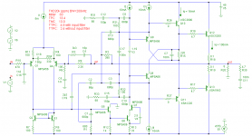
Could you post the full schematic of the simulated "TTPC configuration"?
Yes, see below.
Cheers,
E.
To all,
Disclaimer: This schematic is far from complete. It only demonstrates the principle of TTPC. Furthermore, do me a favor: don't ask me how to fill in all the missing details, as I have no intention to go on with this design.
Attachments
- Home
- Amplifiers
- Solid State
- Bob Cordell Interview: Negative Feedback