...as one owner said to me recently. To my shame I didn't get his approval to quote him but I'm quite confident that he will forgive me! In fact, the whole statement was something like this: " It's the ultimate size! a miniature beauty." Partially I agree with him thought I'm reluctant on "ultimate size" since I know this design can be squeezed furthermore.
Hello guys,
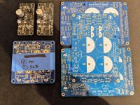
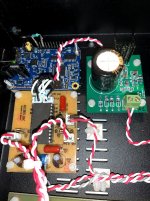
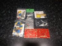
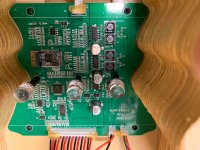
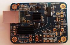
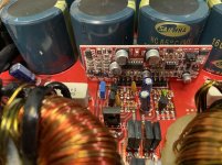
I'm speaking about my latest board called BluWave made from pure love to build something good and affordable. I did spend some
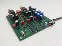
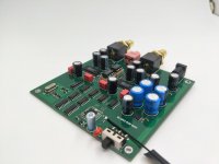
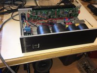
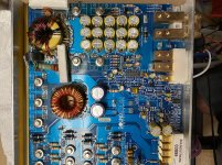
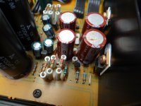
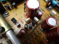
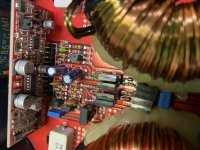
years now to build up this small PCB but I worked occasionally on it. Since I know this post can be edited later on, I'll attach two pictures of a dirty board, top and bottom. I'm sorry that it looks terrible but I'll get back later with updated pics. This board is based on my previous design (Wave IO) but I did make some improvements here and there. For those guys who are thinking about this board to be a second iteration of Wave IO I want to state form the beginning that it does output only SPDIF signal, nothing more! So, there are no I2S buses or something like it... not this time!
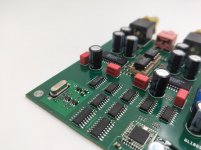
As for this new card, you will easily notice that I've learned the lesson of
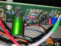
not using pin jumpers when it comes to ... everything. Instead of this I opted out for PCB-designed jumpers, made purely of copper pads and your solder. This allows you to choose a particular configuration without be worried about parasitic resistances which can develop mostly due to moisture. I do confess those PCB jumpers could be small for some of us...
What are those configuration options?
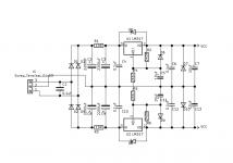
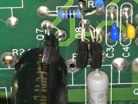
1. The most important one is related to on-board "audio"/main clocks. This board does own a pair of small NDK oscillators used to generate all the clock/data signals for the output SPDIF stream. Using local oscillators is the default configuration for BluWave. Alternatively, a pair of U.FL. coaxial connectors are available in case you like to use your own external clock generators. This external signals should run freely, wired to those two tiny uBNCs: one for 22.5792 MHz (J7) and the other one for 24.576 MHz (J6). The related PCB jumpers to switch the clock sources are JP2 and JP3.
In this mode and to minimize the noise amount, local NDK oscillators can be disabled by cutting default traces to JP5 and JP6 => both oscillators will become dead silent.
2. The second option - which I guess is not so important - is related to on-board LEDs. In case you want to see them disabled then cutting the wire on JP4 will cause all LEDs to stay dark. Regardless of JP4, the signals on closely related pin-header J5 will always be available to drive panel mounted LEDs, for example.
3. JP1 is not used in this hardware revision so please leave it as it is.
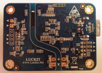
Other than that, this board does have:
* USB input completely isolated form the output side.
* USB receiver + processor powered form USB bus while the output side can be powered separately from whatever external PSU you like. You do also have the possibility to power all the board form USB Bus. Due to some technical limitations, there's
no option to entirely power this board only from your external power source.
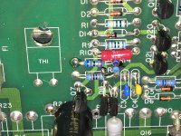
* reclocking stage on output signal's path.
* main NDK oscillators on the "quiet" side.
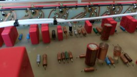
* plenty of filters and decoupling networks.
It's my belief that saying which kind of parts I'm using is simply irrelevant since implementation (layout + part choices) is equally important. Let's say that I did my very best to keep all of them aside one from another trying to minimize the noise on this board and keep it to the lowest possible value I could afford. On the other end, signal integrity was my second concern where plenty of my efforts were spent on making square signals "square", especially for SPDIF output.
The output pin header (J4 - 2.54 mm pitch) is used by this board to share signals with the rest of your system (white arrows will show you the direction of that particular signal: input or output /
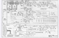
no bidirectional). As usual, PCB is made of four copper layers in 35 / 70 / 70 / 35 um layer stack config as my previous design.
I decided to open this thread to share knowledge and gather feedback about it so I can improve this design along the way. Let's see where it goes!
Update 03-March-2017: After reading
below post I decided to share some of BluWave's key features that I consider worth to be mentioned and bring clarifications where are needed:
* This board does provide SPDIF output only acting solely as USB to SPDIF bridge.
* First choice for a four layer board topology applied to this board was signal's integrity and noise minimization. Signals are properly terminated so the over / under-shoots artifacts are kept to minimum values.
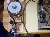
* The power rails for this board are the most addressed parts of this design. This board does have bead filters and plenty of decoupling caps all over the place. Second reason why I choose for 4 layer copper board.
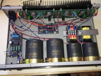
* PSUs are made entirely of linear voltage regulators. Despite the fact that in most cases a small SMPS circuitry will do the trick and be easier to implement, especially for the core voltage of the processor, I decided to use linear Vregs instead regardless of the power dissipation involved. BTW, that is the main purpose for those two glued heatsinks present on this card!
* By default, the output side is completely isolated form the USB receiver. The single exception is where one is wishing to power up the whole board from USB bus. In this particular case, the USB ground layer will be directly shared all across this board. In any other cases, USB grounds (and all related noise) will be kept apart from the rest of audio setup involved.
* Output side consist of SPDIF circuitry + main oscillators + reclocking stage and related PSUs. The Vreg used here does have better specs compared to what I've used on Wave IO. Star power sharing and ground planes will try to preserve the desired low noise levels.
* The ESD trouble was taken into account by applying proper protection circuitry to important nodes.
* BluWave can have two sources for main clock signals: on-board NDK oscillators (finest available to me) and external clocks applied through U.FL. connectors. When external clocks are applied, local oscillators can be disabled... both of them.
* The output data rate can start with 24bit / 44.1 kHz and go up to 24bit / 192 kHz.
* This board comes with
free future support for Windows drivers as many of Wave IO users are used with! And, yes, drivers are genuine! Not something like a hacked copy of "luckit drivers" which you'll find all over the internet! ... drivers that, at origin, were mine too.
* Possibility for future firmware update though USB DFU, in case it's needed.
Update 10-March-2017: I totally forgot to add the price for this board! And, since there are many asking for this info I thought to list it. Before doing that I want to say that all the BluWave boards I have here which are part of my prototype batch will get a 10 Euro discount from the intended price tag (99 Euro). So, pilot boards will carry a price of 89 Euro with Paypal and shipping charges
included in it.
Update 22-April-2017 with board dimensions:
Kind regards,
L


.jpg")


 This thread was split from the
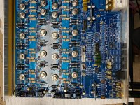


