Active Crossover Volume Control, Stage Ordering, & Board Layout
- By Kellis
- Analog Line Level
- 11 Replies
Good afternoon,
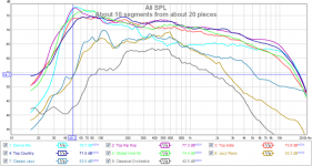
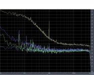
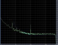
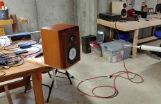
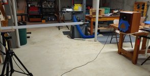
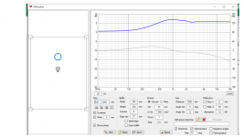
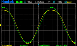
Last year I designed and built a 3-way active crossover network, using circuits pulled directly from the Linkwitz Lab site. The crossover was intended to replace a MiniDSP 2x4 and add outputs for subwoofers. It went together just fine and sounded pretty good, albeit a little warm. Fast forward to a few weeks ago, I was playing with a newly acquired Umik-1 and noticed that there was a definite high-frequency rolloff which is dependent on the position of the potentiometer used for volume control. Below are two traces, one with the pot at 50%, and one at 100%, with the source output level adjusted to give the same volume on the low end. Note that these were taken in my living room on a makeshift mic stand, so they aren't particularly pretty, but they do get the point across.

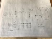
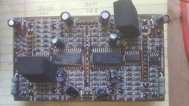
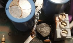
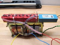
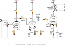
My first instinct was that this was due to the lack of a buffer between the volume pot and the high pass filter for the tweeter, as shown below. However, the rolloff seems to start well below the crossover point (1,250 Hz), with the levels already down ~2 dB at 700 Hz.


Above: Input HPF / buffer and volume pot (left), high pass which takes signal directly from the volume pot (right)
My attempt to solve this would be to add an additional buffer between the volume control and the filter stages, so there is no interaction between the pot and the other passive components involved. Can anyone guess as to whether this might solve the issue?
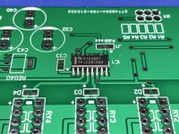
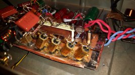
Additionally, if I am going to layout the board again, I wanted some input on the ordering of the filter stages. Linkwitz hints that the order is important on his page, but doesn't offer any advice as to the optimal layout. Here is the how they are currently arranged:

My main question is regarding the shelving low pass for the woofer baffle step compensation, since it is the only stage with a non-unity gain; should it be at the beginning of the woofer filter chain, as shown above, or at the end?
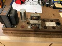
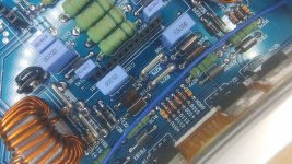
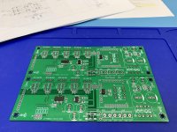
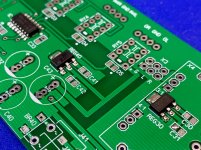
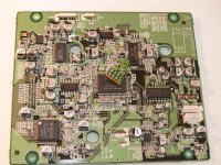
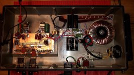
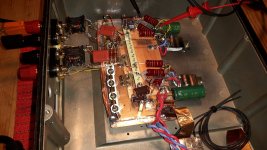
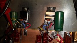
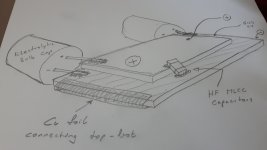
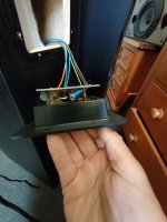
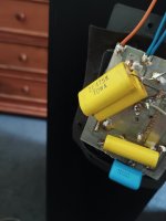
Finally, I wanted some general advice with the PCB layout. I'm not currently experiencing any issues with RF or weird noises, but I'm sure my layout could be improved. The only considerations I had in mind with the design were to put a small filter cap on the V+/V- pins of the opamps, and to try to keep power traces away from signal traces when possible. Here is the layout of the board I went with:


Are there any blatant issues that stick out in the above layout?
As always, thank you for reading and I appreciate any input that y'all might have.
Kellis
Last year I designed and built a 3-way active crossover network, using circuits pulled directly from the Linkwitz Lab site. The crossover was intended to replace a MiniDSP 2x4 and add outputs for subwoofers. It went together just fine and sounded pretty good, albeit a little warm. Fast forward to a few weeks ago, I was playing with a newly acquired Umik-1 and noticed that there was a definite high-frequency rolloff which is dependent on the position of the potentiometer used for volume control. Below are two traces, one with the pot at 50%, and one at 100%, with the source output level adjusted to give the same volume on the low end. Note that these were taken in my living room on a makeshift mic stand, so they aren't particularly pretty, but they do get the point across.
My first instinct was that this was due to the lack of a buffer between the volume pot and the high pass filter for the tweeter, as shown below. However, the rolloff seems to start well below the crossover point (1,250 Hz), with the levels already down ~2 dB at 700 Hz.
Above: Input HPF / buffer and volume pot (left), high pass which takes signal directly from the volume pot (right)
My attempt to solve this would be to add an additional buffer between the volume control and the filter stages, so there is no interaction between the pot and the other passive components involved. Can anyone guess as to whether this might solve the issue?
Additionally, if I am going to layout the board again, I wanted some input on the ordering of the filter stages. Linkwitz hints that the order is important on his page, but doesn't offer any advice as to the optimal layout. Here is the how they are currently arranged:
My main question is regarding the shelving low pass for the woofer baffle step compensation, since it is the only stage with a non-unity gain; should it be at the beginning of the woofer filter chain, as shown above, or at the end?
Finally, I wanted some general advice with the PCB layout. I'm not currently experiencing any issues with RF or weird noises, but I'm sure my layout could be improved. The only considerations I had in mind with the design were to put a small filter cap on the V+/V- pins of the opamps, and to try to keep power traces away from signal traces when possible. Here is the layout of the board I went with:
Are there any blatant issues that stick out in the above layout?
As always, thank you for reading and I appreciate any input that y'all might have.
Kellis