Cadence M4000 class D full range 4-channel Korean amplifier:
Problem: When powered up, no load, amplifier in protect mode. Every 4 seconds amp attempts to power up automatically then immediately goes back in protect mode.
What I have found:
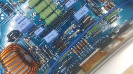
Through checking with multimeter, Channel 1 output fets (19n20 and 17P10) shorted. One trace burnt (between D118 and C169 in picture).
What I have done:
Removed rectifiers, powered up via variable voltage low amperage P.S. and the power supply section looks fine. square wave (+14v on power supply fets) and + 30v/ -30v on rectifier pins. All fets cool, idling fine with power led on and no protect mode.
Fixed the trace by soldering in solid copper jumper wire. Pulled diode D118 and it checked good also checked C169 and it was the same as all other capacitors of the same value. All other resistors seem to be within tolerance.
Should I be able to replace the two shorted output fets and test it or should I test the output driver board? If there is a bad component on the driver board could it cause a failure of the output FETs?
Which brings me to my questions about the driver board.
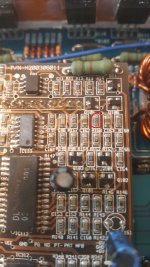
The numbers on the ICs have been removed. The one IC that is a 28 pin, I can not find anything like it, other than the y-tech IC in the tutorial, but that is not really like it either. Does anyone have an idea what the number could possibly be? It seems like one side (14 pins) pertain to channel 1 and the opposite side pertains to 2 when following the traces. The same with channels 3 and 4 on the other end of the board.
Also any idea of the 14 pin IC next to it?
The 8 pin dual comparator is a A393F.
Also there are two types of driver transistors I am assuming P and N that are labeled under "Qn.." {n=1 to 4}, "ZH C0" (only thing I can find with that nomenclature is a HSMS-2820 Schottky diode, but I don't think that is correct) and "ZG C8" (maybe BCF30 PNP transistor?) and another labeled "Dn.." {n=1 to 4}, "F3 J8" (maybe a BCX71JR, BJT transistor connected as a diode?)
Also does anyone have a schematic that would be close to this "Asian clone" amp.
The amp uses:
IRFZ-46N PS FETs
FQP17P10 and FQP19N20 output FETs
KIA7806A and KIA7906PI +/- 6V voltage regulators
KIA7815A and KIA7915PI +/- 15V voltage regulators
FMG22R and FMG22S rectifiers
Lastly is Newark a good place to buy the 17P10 and 19N20 FETs from? Digi-key and Mouser are out of stock on the 17P10.
Thank you in advance.
Problem: When powered up, no load, amplifier in protect mode. Every 4 seconds amp attempts to power up automatically then immediately goes back in protect mode.
What I have found:
Through checking with multimeter, Channel 1 output fets (19n20 and 17P10) shorted. One trace burnt (between D118 and C169 in picture).
What I have done:
Removed rectifiers, powered up via variable voltage low amperage P.S. and the power supply section looks fine. square wave (+14v on power supply fets) and + 30v/ -30v on rectifier pins. All fets cool, idling fine with power led on and no protect mode.
Fixed the trace by soldering in solid copper jumper wire. Pulled diode D118 and it checked good also checked C169 and it was the same as all other capacitors of the same value. All other resistors seem to be within tolerance.
Should I be able to replace the two shorted output fets and test it or should I test the output driver board? If there is a bad component on the driver board could it cause a failure of the output FETs?
Which brings me to my questions about the driver board.
The numbers on the ICs have been removed. The one IC that is a 28 pin, I can not find anything like it, other than the y-tech IC in the tutorial, but that is not really like it either. Does anyone have an idea what the number could possibly be? It seems like one side (14 pins) pertain to channel 1 and the opposite side pertains to 2 when following the traces. The same with channels 3 and 4 on the other end of the board.
Also any idea of the 14 pin IC next to it?
The 8 pin dual comparator is a A393F.
Also there are two types of driver transistors I am assuming P and N that are labeled under "Qn.." {n=1 to 4}, "ZH C0" (only thing I can find with that nomenclature is a HSMS-2820 Schottky diode, but I don't think that is correct) and "ZG C8" (maybe BCF30 PNP transistor?) and another labeled "Dn.." {n=1 to 4}, "F3 J8" (maybe a BCX71JR, BJT transistor connected as a diode?)
Also does anyone have a schematic that would be close to this "Asian clone" amp.
The amp uses:
IRFZ-46N PS FETs
FQP17P10 and FQP19N20 output FETs
KIA7806A and KIA7906PI +/- 6V voltage regulators
KIA7815A and KIA7915PI +/- 15V voltage regulators
FMG22R and FMG22S rectifiers
Lastly is Newark a good place to buy the 17P10 and 19N20 FETs from? Digi-key and Mouser are out of stock on the 17P10.
Thank you in advance.
Attachments
Last edited:
Possibly:
http://www2.kec.co.kr/data/databook/pdf/KTN/Eng/KTN2907U_AU.pdf
http://www2.kec.co.kr/data/databook/pdf/KTN/Eng/KTN2222U_AU.pdf
http://www2.kec.co.kr/data/databook/pdf/KDS/Eng/KDS193.pdf
Newark is OK but you have to watch the location. Sometimes the stock is in Europe and will incur excessive postage.
I don't know what the 14p IC is. The large IC may be a DLI4060B. That's what's used on the Planet Audio BB175.4B. It's roughly similar.
Perry,
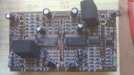
I found a pic of the PA BB175.4B and both amps are very similar on the inside.
Do you have a data sheet for the DLI4060B? I had no luck finding one.
Thanks for the data sheets for the transistors and diode.
The output FETs are on order. When they arrive should I just put the new FETs in along with the driver board and see what happens or should I attempt to, given that I have no pinouts for the two ICs, check the driver board components before hand?
Is it okay to the power up the amp with the driver board installed and the output FETs in three channels, while the channel 1 FETs are removed?
Thank you
I'd try powering up the amp with 3 channels functioning and see what the drive looks like for the 4th channel (after replacing the known bad driver components).
You can use the working channels to find the output pin on the IC or the driver board headers. That should let you check the condition of the drive before the driver transistors.
I was wrong about the ICs being 4060s. They may be 4050s. See attached.
You can use the working channels to find the output pin on the IC or the driver board headers. That should let you check the condition of the drive before the driver transistors.
I was wrong about the ICs being 4060s. They may be 4050s. See attached.
Attachments
Thank you Perry. I do agree that the 28 pin IC is a DLI4050. Also the transistors are the same as the data sheets you uploaded.
I now have the amplifier running without going into protection after changing several shorted zener diodes and the low and high side FETs on CH 1. Three channels are working well but CH1 is still just producing static.
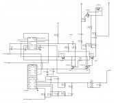
I have traced the components down on the driver board and attempted to place them in a schematic. My first attempt at drawing electrical schematics, so if anything does not look right let me know.
I am pretty sure the problem is that the 14 pin IC, "IC113" in the picture of post 1, is not generating the triangle wave at all on pin 5 and a poor square wave on pin 12 for channel 1. Pins 10 and 7 work fine for channel 2. Of course the markings are gone from the IC and I am having no luck finding an IC with the same pinout. It may be another proprietary IC made by DLogixs, I don't know. Does that IC look familiar to anybody? Any suggestions on something that might work in its place? Would a function generator or oscillator be the correct name for it?
I now have the amplifier running without going into protection after changing several shorted zener diodes and the low and high side FETs on CH 1. Three channels are working well but CH1 is still just producing static.
I have traced the components down on the driver board and attempted to place them in a schematic. My first attempt at drawing electrical schematics, so if anything does not look right let me know.
I am pretty sure the problem is that the 14 pin IC, "IC113" in the picture of post 1, is not generating the triangle wave at all on pin 5 and a poor square wave on pin 12 for channel 1. Pins 10 and 7 work fine for channel 2. Of course the markings are gone from the IC and I am having no luck finding an IC with the same pinout. It may be another proprietary IC made by DLogixs, I don't know. Does that IC look familiar to anybody? Any suggestions on something that might work in its place? Would a function generator or oscillator be the correct name for it?
Attachments
Last edited:
I found the attached diagram after my last post in this thread. It's likely similar to yours.
When drawing a diagram, the components that are connected to the positive voltage sources are generally above the ones that are connected to ground or the negative supply. There's no reason to redo your diagram.
I don't have a source for the IC. You could try contacting the 'manufacturer':
Contact Us – Cadence Sound
Attachments
The DL201, IC2A and IC2B, in the schematic you provided appear to be the same pinout and function as the IC in question. Cadence has been of no help and DLogixs email on their website is not valid. I cannot find anything on a DL201 while searching.
If the pins for the bad part of the original IC were cut, then an external function generating IC i.e. a ICL838, was connected to the correct pads with jumper wires could that work to provide the missing input to the DLI4050 comparator and the output FETS?
I would assume that the frequency and duty cycle of the outputs on a good channel could be determined with an oscilloscope and then look for a IC within those parameters.
What would be the proper way to inject the signals into the circuit using a UTG932 function generator to test that the proper outputs would indeed fix the channel? In the Advanced Class D Testing it mentions a film capacitor placed in series with the input for protection of the function generator, but I am not sure I understand if the point 5 in the diagram is for the input of the IC or the output.
I will try the LM319, but will have to order a few. I do have on hand some KA339 Quad Comparators. Do you think that would work for testing?
If I wanted to use a benchtop 2 channel function generator, if the idea of injecting the signals at the outputs of the DL201 is reasonable, how would I connect the FG to the outputs minimizing any risk of damaging the FG?
I believe there is a short in the DL201 IC on the triangle wave output, because I am getting -6Vdc on the output that is not on the other three working channels.
Should I lift the pins of the DL201 where I want to inject the signal and connect to the pads of the circuit or is it okay to connect to the output pins of the IC?
Thanks
If the DC voltage on the injection point is the same as that of the generator, a resistor of about 1k should protect the generator. Many generators have a series 50 ohm resistor and can drive into a dead short without damage.
If you lift the output terminal of the comparator, you should be able to inject a signal.
The pin configuration of the 339 is significantly different. I don't know if it will work.
Is the output of the comparator a triangle waveform? I would expect it to be a square wave at that point.
If you lift the output terminal of the comparator, you should be able to inject a signal.
The pin configuration of the 339 is significantly different. I don't know if it will work.
Is the output of the comparator a triangle waveform? I would expect it to be a square wave at that point.
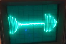
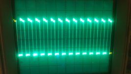
I will get pictures of the waveforms on the oscilloscope and post them. On the working channels, on the DL201, pins 7 and 12 there is a square wave output of 12Vpp. On pins 5 and 10 there is an high frequency triangle wave output of 1 Vpp.
Not sure if this is correct, but my thinking is that the triangle wave is input for the DL4050 to compare to the input from the sinewave from the preamp/source to build the PWM signal. The square wave is sent to drive the output FETs. Does this sound right?
Not sure if this is correct, but my thinking is that the triangle wave is input for the DL4050 to compare to the input from the sinewave from the preamp/source to build the PWM signal. The square wave is sent to drive the output FETs. Does this sound right?
I am back at this one again. I am to the point of swapping parts/ICs, but before I do I thought I would post post a couple of pictures of the drive signal I am getting on the drain of the output FETs of the the bad channel left and good channel right. Hopefully this bad signal looks familiar to a problem someone else has had in the past.
I do not have a good triangle wave to be input to the comparator on the bad channel. Still not sure if the problem is one of the ICs (DLI4050B2 and DL201) or components in the drive or feedback circuits.
I have managed to get audio out of the bad channel but it is attenuated with respect to the other channels and has quite a bit of static on it.
Attachments
While poking around I found that when I put my finger across the 22k resistor the audio clears up. I then, with a current limiting bulb in series with b+, when I probe across the resistor with the leads of the dmm turned off the channel clears up. If I turn the meter on to check voltage across the resistor the amp draws excessive current. I took the current limiter out so that I could get an idea of the current it was drawing and now the amp is in protection mode with at least one output fet blown.
After I get the amp out of protection, what could be causing the channel to work while touching the resistor?
After I get the amp out of protection, what could be causing the channel to work while touching the resistor?
Attachments
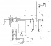
What resistor does your resistor correspond to on the 4150 diagram?
Is the 22k resistor within tolerance?
Does it have a capacitor in series or in parallel with it that's out of tolerance?
Is the 22k resistor within tolerance?
Does it have a capacitor in series or in parallel with it that's out of tolerance?
It is R156, circled in red in the picture.
It is located in the upper right hand portion of the drawing and connected to both emitters of Q105 and Q106.
It is in tolerance (22K), checked in circuit.
I checked all capacitors on that channel (on the driver board) and compared them to the corresponding caps on the other channels on the driver board. Checked with an ESR meter while in circuit. The majority of caps are surface mount with no marking as to values.
I'm guessing it's R24C.
Does the software you used have 'rubber bands' to allow you to reposition parts without breaking the connections?
If you lay tape over the resistor, does touching it through the tape make a difference?
If you tape off ALL of the other local components so you can ONLY touch that resistor, does it still change the way the amp functions when you touch the resistor?
I don't understand what is meant by R24C.
Are you referring to the software I used to draw the circuit diagram? If so I don't remember which one it was, it was a free one I found on the internet. I will look and see if I can figure out what the name of it was.
When I put the dmm probes across the resistor with it set to Vdc, the amp suddenly drew a lot of current and destroyed an output fet at the least and amp is now in protect and will not run. I will try and get it back running and then try the different steps using the tape.
It's in the diagram I posted in post #6.
I don't need to know the name. I was simply asking about the features. The diagram would be much easier to read if it was more like the diagram I posted.
I don't need to know the name. I was simply asking about the features. The diagram would be much easier to read if it was more like the diagram I posted.
I see, yes it looks like it corresponds to R24C. The surrounding resistor values in the EA4150D diagram are different than what is on the driver board that I have but there are defiantly similarities to the board I have.
When I drew it, It is obvious that I didn't know what I was doing, I just tried to have some way to keep up with all the connections and values. I drew it out in a way that mimics how the components are literally laid out on the board.
I will see if I can re draw it to better match the EA4150D diagram.
I was thinking if I can figure out the name of the program, I could then look it up and determine the features associated with it.
Last edited:
- Home
- General Interest
- Car Audio
- Cadence M4000