All,
I would like to share with you the experience I got with a Chinese version of the AMB Sigma 11.
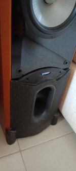
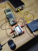
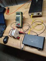
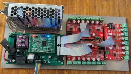
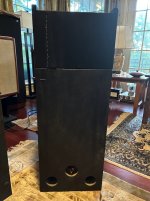
I didn't know the existence of the AMB sigma 11 project thus many months ago I went to Ebay to find out a good-and-cheap LPS to supply my Allo USB Bridge and Chord Mojo.
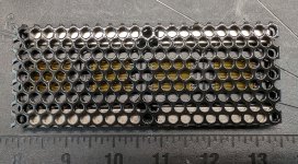
I found this unit:
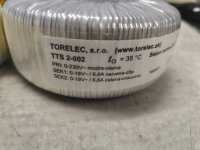
ZEROZONE Super-PSU 30VA DC5V 2A Alimentatore LPS Linear per fonti audio | eBay
This was enough expensive to make me think this was a good one.
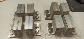
Few days ago a friend of mine that is helping me modifying my Mojo with supercaps (the battery died) suggested me to implement the Sigma 11 LPSU since it would perfectly fit with my equipment.
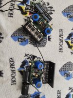
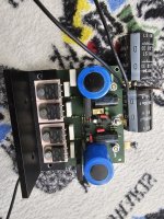
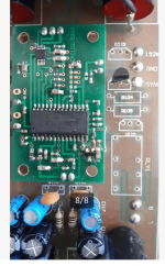
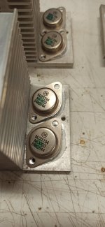
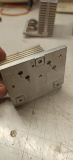
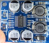
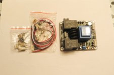
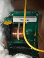
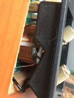
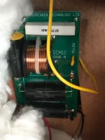
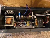
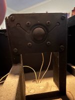
At a first sight I identified the PCB of my LPSU was pretty similar to the sigma 11 project.
Actually I discovered there are some Chinese traders that are selling SIGMA 11 modified board without any license.
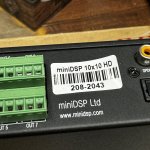
Vary bad. Shame on me since I bought one.
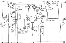
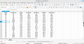
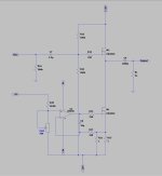
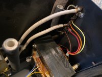
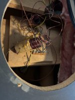
Now I spend some time to draw the electric schema of such unit.
Please find it below. (in grey the original component value as per Sigma 11 project).
Beside the component quality that is pretty high (Nichicon capacitor, given they are genuine...I cannot say that), the schema - attached - has been changed in few parts.
Let me list for you:
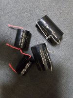
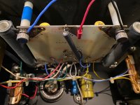
1. C18 (secondary filter right before the output) is now a 3300mF (even if the PCB is indicating a 10000mF capacitor) electrolytic capacitor (should be a 1mF polyester)
2. The gain of the regulator output is obtained with a 4.3V Zener * R8/(R10+Trimmer) = about 1.3. I suppose they introduced the trimmer to slightly adjust the output voltage. The original schema suggested a 5.1V zener and R10 not installed (Gain =1) for a shorter and simpler schema.
3. C14 3n3 instead of 3n9. My guess here is they just finished the 3n9 and put a 3n3 capacitor...
4. C13 has been lowered to 47mF instead of 100mF. This is part of an RC filter with R3 (1k as per original schema) to lower down the zener noise. Sincerely this seems to be a go-for-a-cheap solution...
5. C11 and C9 lowered down to 100mF and 47 mF instead of the original 470mF and 100mF. They are filtering the voltage reference and line regulation. go-for-a-cheap-solution even in this case?
6. C5 the input filter capacitor has been lowered to 4700mF to 3300mF (even if the PCB is indicating a 10000mF capacitor)
7. rectifier diodes are MUR 1560 instead of MUR 820. Actually they are a bit slower (60 ns vs 35ns ) than the original but they have an higher Vf since they drain about 1.5 V MAX each instead of 0.9 MAX. This could the reason why they chose to have a 12V secondary voltage (through a cheap R-Core Xformer) instead the suggested 9V to obtain 5V output.
Overall they increase the output filter from 1mF to 3300mF (or 10000mF as per PCB indication) but they reduced the filtering of the internal PSU stages (voltage reference and error amplifier). Unfortunately I do not have an oscilloscope thus I cannot say how low-noise is the output.
What do you think?
Would it worth to change back all the modified components to fit the original schema?
Thank you in advance to whom would like to help on this topic.


.JPG")
.JPG")
.JPG")

.JPG")