

DIY Audio Analyser using CS4398 / CS5381 - UPDATE!
Posted 15th November 2015 at 09:05 AM by googlyone
I have more or less completed the audio analyser based on CS4398 and CS5381.
In an earlier post I suggested I had reached the limits of these IC's. I was wrong. What I had reached the limit of was getting the grounding "OK" for a single (unbalanced) input measurement system.
I have since built a balanced front end - in fact I simply built a Silicon Chip PCB as it was pretty well what I would do - and integrated this to the ADC and DAC.
It looks a bit like this:
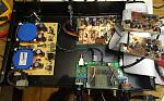
What you see is:
- On the left are two independent power supplies
- In the back middle is a MiniDSP USB Streamer card.
- In the middle back is an interface card that
- Does optical isolation of the MiniDsp USB Streamer
- Does more regulation for the ADC and DACs
- Generates local clocks for the DAC and ADC
- Feeds these back to the MiniDSP Streamer
Hanging on one of the ribbon cables is the CS4398 DAC. And on the other is the CS5381 ADC.
In the middle at the front is the Silicon Chip balanced interface. The Silicon Chip (an Australian hobbyist magazine) implementation used a rotary switch for the attenuator. I hate these things with a vengeance for audio, as I have too many years of replacing switches as they become noisy.
So instead I use a rotary switch to drive relays to switch the attenuators. I built the PCB to line up exactly with the holes on the Silicon Chip card. It works nicely. I imagine that the Silicon Chip implementation avoided relays as they get expensive when you throw a dozen of them at a problem.
A few comments:
- The balanced line input works pretty well. It uses four paralleled NE5532 op amps rather than a single one in the balanced receiver stages to keep noise down. It seems to work - though after I had built it I realised I had a tube of LM4562's sitting right in front of me!
- The CS4398 DAC uses completely independent filters and a separate balanced to single ended converter. I put a lot of effort into getting this right, as the single ended DAC appeared to be a limitation in previous tests.
- The CS5381 ADC again uses independent drives - and is much more reminiscent of the AKM app note than the CS one I originally took guidance from.
So how does it go?
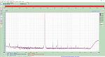
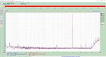
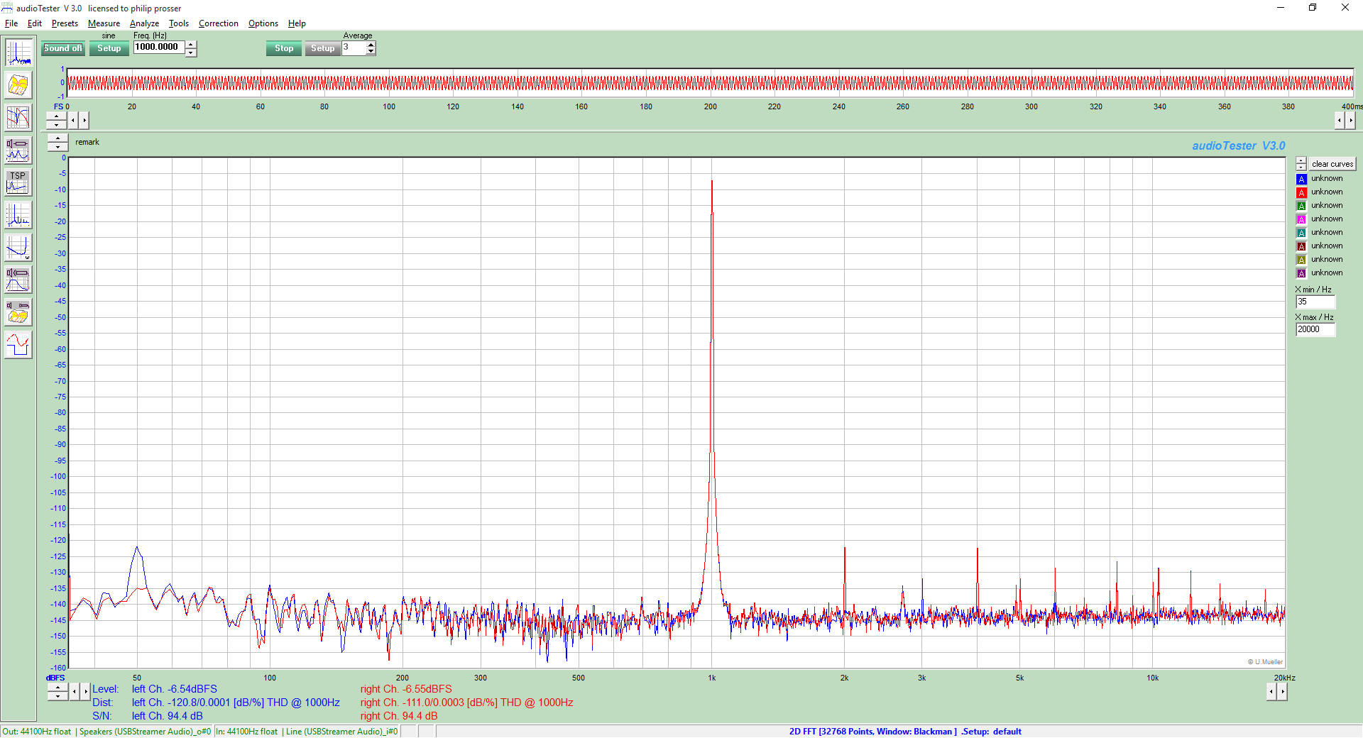
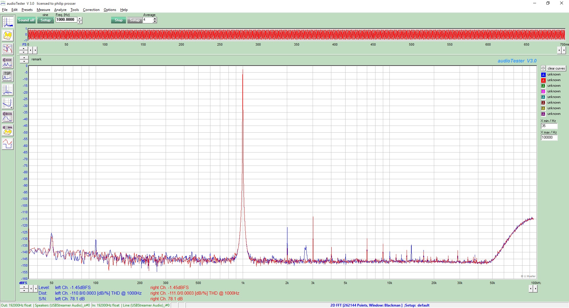
- Much of my work was at 48k samples/sec, as this is the sample rate of my DSP crossover. This is the 1KHz loopback at -6dB

I was pretty chuffed with this. After all the hassles I have had, I wondered if this was a fluke. I set to work 6 more ADC boards and tried them out - they were all broadly similar to this, with minima of loopback distortion in the 0.0001 to 0.0002%. Interestingly, the right channel appears more likely to give higher distortion than the left. I still think this is most likely inherent in the device.
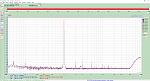
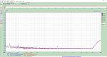
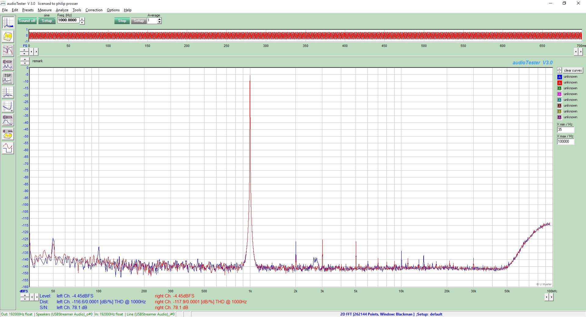
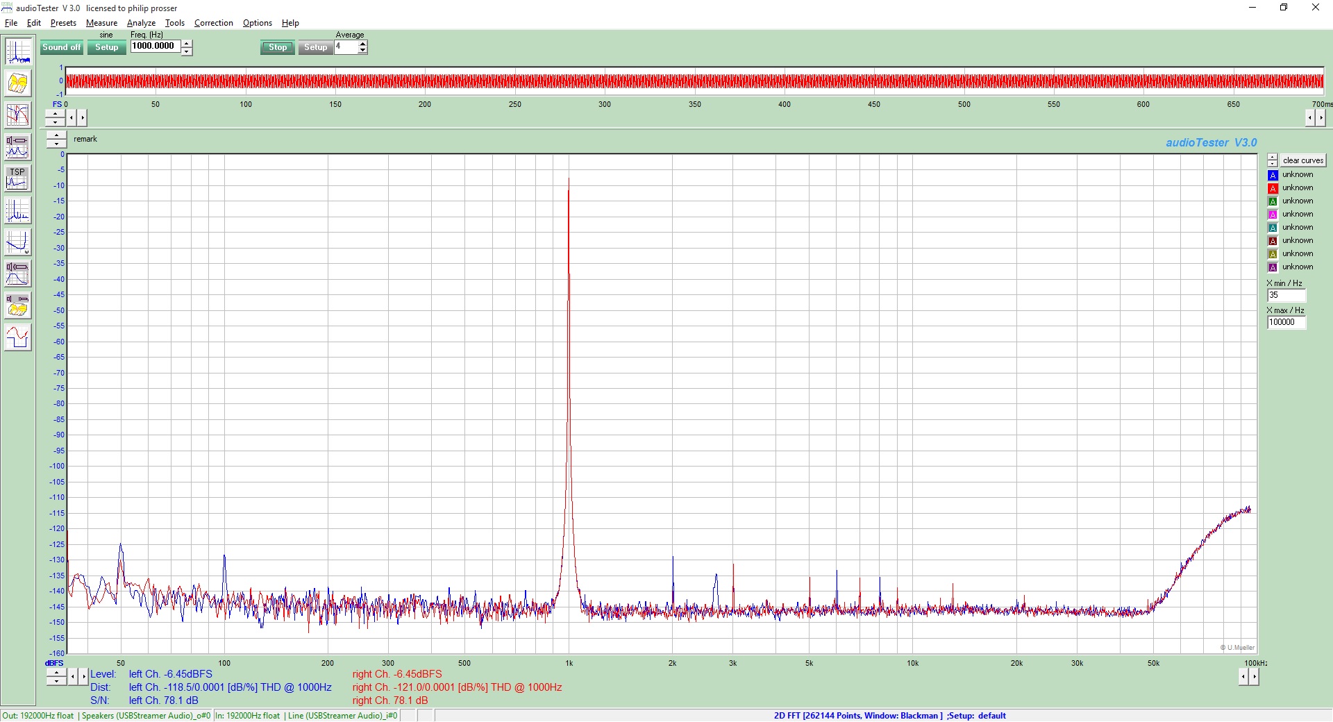
Today I rejigged the mode select pins on the ADC and DACs to 192ks / sec. This is the results..
At -1dB, this is about as high as you would want to go...
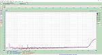
at -4dB:
At -6dB:
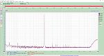
Again, I am pretty chuffed. I need to look into the increasing noise floor above 50kHz - I suspect this is a property of the CS5381.
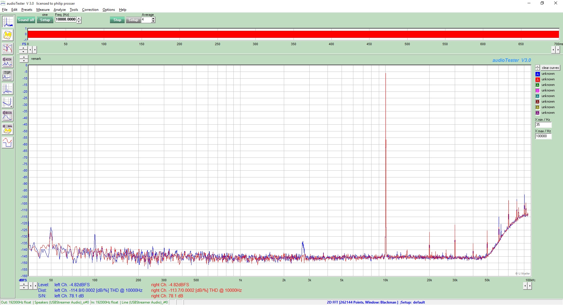
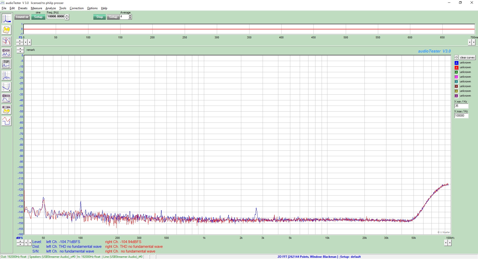
So how does it go at 10kHz?
I think this is pretty OK.
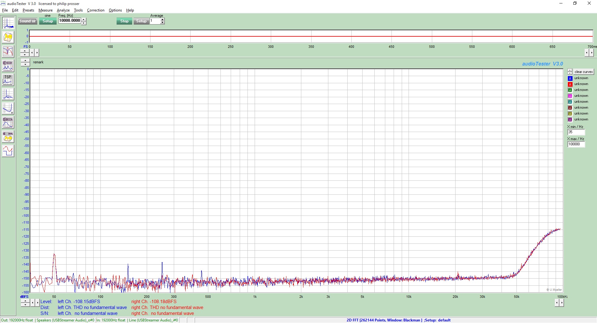
And the noise floor?
With the DAC generating silence:
and with 40dB attenuation on the differential receiver:
Now I need to package it all up and get on with testing the amplifier that kicked me off on all this!!!!
In an earlier post I suggested I had reached the limits of these IC's. I was wrong. What I had reached the limit of was getting the grounding "OK" for a single (unbalanced) input measurement system.
I have since built a balanced front end - in fact I simply built a Silicon Chip PCB as it was pretty well what I would do - and integrated this to the ADC and DAC.
It looks a bit like this:

What you see is:
- On the left are two independent power supplies
- In the back middle is a MiniDSP USB Streamer card.
- In the middle back is an interface card that
- Does optical isolation of the MiniDsp USB Streamer
- Does more regulation for the ADC and DACs
- Generates local clocks for the DAC and ADC
- Feeds these back to the MiniDSP Streamer
Hanging on one of the ribbon cables is the CS4398 DAC. And on the other is the CS5381 ADC.
In the middle at the front is the Silicon Chip balanced interface. The Silicon Chip (an Australian hobbyist magazine) implementation used a rotary switch for the attenuator. I hate these things with a vengeance for audio, as I have too many years of replacing switches as they become noisy.
So instead I use a rotary switch to drive relays to switch the attenuators. I built the PCB to line up exactly with the holes on the Silicon Chip card. It works nicely. I imagine that the Silicon Chip implementation avoided relays as they get expensive when you throw a dozen of them at a problem.
A few comments:
- The balanced line input works pretty well. It uses four paralleled NE5532 op amps rather than a single one in the balanced receiver stages to keep noise down. It seems to work - though after I had built it I realised I had a tube of LM4562's sitting right in front of me!
- The CS4398 DAC uses completely independent filters and a separate balanced to single ended converter. I put a lot of effort into getting this right, as the single ended DAC appeared to be a limitation in previous tests.
- The CS5381 ADC again uses independent drives - and is much more reminiscent of the AKM app note than the CS one I originally took guidance from.
So how does it go?
- Much of my work was at 48k samples/sec, as this is the sample rate of my DSP crossover. This is the 1KHz loopback at -6dB
I was pretty chuffed with this. After all the hassles I have had, I wondered if this was a fluke. I set to work 6 more ADC boards and tried them out - they were all broadly similar to this, with minima of loopback distortion in the 0.0001 to 0.0002%. Interestingly, the right channel appears more likely to give higher distortion than the left. I still think this is most likely inherent in the device.
Today I rejigged the mode select pins on the ADC and DACs to 192ks / sec. This is the results..
At -1dB, this is about as high as you would want to go...
at -4dB:
At -6dB:
Again, I am pretty chuffed. I need to look into the increasing noise floor above 50kHz - I suspect this is a property of the CS5381.
So how does it go at 10kHz?
I think this is pretty OK.
And the noise floor?
With the DAC generating silence:
and with 40dB attenuation on the differential receiver:
Now I need to package it all up and get on with testing the amplifier that kicked me off on all this!!!!
Total Comments 4
Comments
-

 Nice work!! I have a much simpler project that I've been meaning to do, just a balanced to single ended (and vice versa) box to put between my focusrite 2i2 and whatever I want to test. I don't think I will be able to reach these performance levels!
Tony.Posted 9th December 2015 at 02:04 AM by wintermute

-
Tony,
I don't see why you shouldn't give it a crack.
The Focusrite specs look reasonable (-100dBc promised - looks like hey use a Cirrus Logic ADC, you might get much better).
I also note they spec it at -1dBc, if the device is similar to the CS5361/81, you will find it delivers better THD at about -10dBc.
In working on the balanced to single ended box, you have hit on a very important part of the measurement system. This will deliver you a great return for the effort you invest.Posted 11th December 2015 at 08:43 AM by googlyone
-
 Hello, googlyone
Looks like you succeed to create an very good instrument.
Do you planning to make the schematics, and PCB or gerbers available ? I'm interesting to build one for myself.Posted 19th December 2015 at 07:56 PM by Tolik
-
Tolik,
I will post the schematics and Altium files for the final boards.
The interface of the MiniDsp to the board is in this implementation fixed to a single sample rate. Jens has a very neat design that allows the system to track any sample rate, but as I use this for test only, so I didn't use that approach.
If you want a more versatile PC interface contact jens for his isolated interface for the MiniDsp.
I get the feeling that jens will be selling his gear, so I can't publish his work, which he provided to me in confidence.
I am on holidays for a couple of weeks, but when I get back I will post the work I have done.Posted 25th December 2015 at 04:28 AM by googlyone

