I haven't read tentalbs's article yet but this: Grounding of Mixed Signal PCBs and few others found with google. I thought to add smd ferrite beads as well, but I will add definitely and I read some other practical tips in tetlabs's article that I will follow... thanks.Hi Vzs
Your groundplane management is the way to go.
You surely looked at tentlabs decoupling note : may be you can add smd ferrite bead at each digital VD input
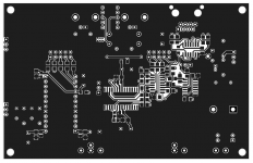
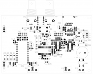
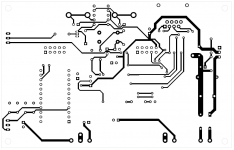
DAC v0.7
Thanks to rtd's recommendation I read tentlabs's document (Supply_decoupling.pdf) and followed their words. Check out the latest schema and pcb design.
I added the digital power supply to the board as I think that a single LM317 does the job. For the sensitive analog supplies everybody (who might build this board) could use its preferred regulator, I will use Salas reg V1.0 with Quanqhao's board.
The ground of each analog supply is connected to the ground plane at the terminal input and the digital ground is connected to the ground plane only near C25. Is this OK?
Cheers,
Zsolt
p.s. Of course I share all this for DIY ONLY
Attachments
Last edited:
Thanks! but I don't think I completely understand what you mean: you suggest to replace 317 with TL431?That is very good! shrugged the source of your charges too extrusion 317 of this AD1865 circuit design! Contacts can be used to replace it Tl431! better!
According to tnt-audio measurements the noise of TL431 is just slightly better then 317: tnt-audio article. The common digital supply has to have enough current for the CS and AD digital parts and for up to 15 logic ICs when the complete I2S converter is used. Probably 100mA is more than enough but I don't want to use TL431 to its maximum ratings.
Hope you will do a Group Buy!p.s. Of course I share all this for DIY ONLY
After the r&d on my side will be successfully finished I might make one.Hope you will do a Group Buy!
I will start working on the converter boards. I will make a simple one with only one inverter for LSBJ to AD and a complete one for I2S to AD. I do this in the idle time of my full time job, so cannot schedule

Anyway, if anybody is interested testing one of these prototypes I could send the files to make the pcbs.
After the r&d on my side will be successfully finished I might make one.
I will start working on the converter boards. I will make a simple one with only one inverter for LSBJ to AD and a complete one for I2S to AD. I do this in the idle time of my full time job, so cannot schedule
Anyway, if anybody is interested testing one of these prototypes I could send the files to make the pcbs.
please sent to me!
thank!
Quanghao
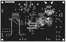
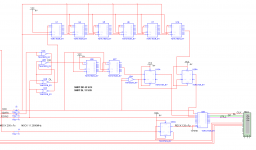
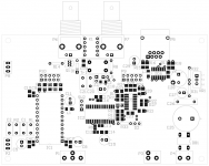
VZ NOS DAC v1.0
Here comes the first test ready version. All component sizes are checked and fit well. I will post a BOM later.
I added capacitor coupled SPDIF input, using J1 and J2 jumpers one might either use a pulse transformer or use small 5mm caps (Wima FKP2) and leave out the pulse transformer.
Next will come the conversion modules: a simple one with one inverter for testing and a complete, re-clocked I2S later.
@Quanghao: On Monday I send you the pcb files
Cheers,
Zsolt
Attachments
Last edited:
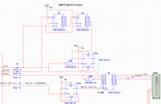
I will connect a converter board between P9, P10 with the schematics attached. It is based on a schematics posted by sampler plus I added reclocking to have everything in perfect sync (reclocking ideea taken from Eric Juaneda's converter board).Vzs,
how you convert the I2S to AD1865 input ?
At least in simulation it converts an I2S signal to perfect AD1865 format.
Attachments
I2S simple
I will try with this simpler I2S converter first for testing. This keeps the 11.34us delay but converts I2S to LSBJ. It contains the same reclocking mechanism as the previously shown one.Vzs,
how you convert the I2S to AD1865 input ?
Attachments
What you mean by true I2S input?So, in your DAC board the I2S input is not a pure I2S input
As you can see in the schematics from post #289 'DAC v1.0.pdf' the board contains an I2S input (P5 - RJ45 connector) which is first buffered (74HC125) then connected to a multiplexer (74HC257) with I2S coming from CS8414. This multiplexed I2S is then routed to AD1865 through the converter board.
Later edit:
You can use this truth table for P8 to switch between I2S and SPDIFs like this:
P8 1 2 3
P5 0 0 1 I2S
P6 0 0 0 SPDIF 1
P7 0 1 0 SPDIF 2
I just found an errata in the schematics. Pin 15 of IC5 (74HC257) should always be connected to ground. I will post a corrected schematics later.
Last edited:
A pure I2S input must follows the I2S standard
to be compatible with device like the CD-PRO transport
DAISy : CD-Pro2 module VAU1254 (CD)
and USB to I2S converters
http://focus.ti.com/lit/ds/symlink/pcm2707.pdf
The AD1865 have a 18 Bits LSBJ input.
On you board you should be specified the necessity of an external circuit to get a true I2S input.
My board does not need external circuit to get true I2S input as it follows the I2S standard of CS8414 which is similar to PCM2707.A pure I2S input must follows the I2S standard
to be compatible with device like the CD-PRO transport
DAISy : CD-Pro2 module VAU1254 (CD)
and USB to I2S converters
http://focus.ti.com/lit/ds/symlink/pcm2707.pdf
The AD1865 have a 18 Bits LSBJ input.
On you board you should be specified the necessity of an external circuit to get a true I2S input.
According to 'DAC v1.0.pdf' the I2S input P5 has the following pin arrangement for I2S signals:
pin 1 - FSYNC (LRCK left/righ channel latches)
pin 2 - SCK (32xfS / channel or 64xfS / stereo sample)
pin 3 - MCK (256xfS)
pin 4 - SDATA (LR data according to I2S format)
pin 5-8 - GND
These I2S signals are routed to the converter board which contains either the simple or the complete I2S converter to 18bit LSBJ of AD1865.
Why do you think a middle circuit would be needed between an PCM2707 board with I2S out and my DAC board?
Later edit:
Anyway, I'm in the middle of the development and hopefully in a month I can try the whole. Beside my work and personal life I have little time for my hobby. I do this only for pure hobby so no commercial interests or competition with other DAC board. I just want to do it in my way.
If you think I hijacked your thread with the development of my DAC board I will start a new thread for it.
Zsolt
Last edited:
If you are thinking that a daughter board is also needed to have I2S conversion, I did specified this in the first post of the development of this DAC board: #280On you board you should be specified the necessity of an external circuit to get a true I2S input.
"The daughter board that will be connected between P9 - P10 (in 90 degree angle) might contain from a simple inverter (to match LSBJ signals from CS8414 to AD1865) to a fully featured I2S converter."
I don't think of the daughter board as external circuit as it is part of the whole project. Anyway, I specified the converter board in all my previous posts. I wanted to do like this (use daughter board) to try out different converters between CS8414 and AD1865, from a simple inverter to see if the whole is working to different I2S converters (those two posted).
Last edited:
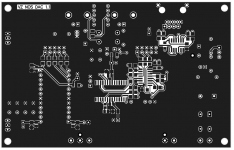
VZ NOS DAC v1.1
Hi! Yesterday I found an error in v1.0 and corrected it: see errata below.
Errata for v1.0 : changed 74HC125 to 74HC126, so no inverter is needed to enable buffer output. Removed the 74HC04 as the in phase/out phase selector will be placed on the conversion board. The whole board became more simple and the ground plane more compact.
!!!! To prevent any confusions keep in mind that neither this nor the previous DAC boards will not work without an I2S - 18 bit LSBJ daughter board connected to P9 - P10 !!!!
I will start the pcb design for the simple I2S - 18 bit LSBJ daughter board (see post #293) asap and will post it.
Zsolt
Attachments
Last edited:
Ad1865 by me is a great chip, and natural sound close to anlalog
Using I2S for AD1865 can not be, and Ad1865 will be able to use 24bit. I'm also working on a version using the I2S and USB inputs for ad1865, when results will be reported later.
I'll try previous versions of VZS.
Using I2S for AD1865 can not be, and Ad1865 will be able to use 24bit. I'm also working on a version using the I2S and USB inputs for ad1865, when results will be reported later.
I'll try previous versions of VZS.
- Status
- This old topic is closed. If you want to reopen this topic, contact a moderator using the "Report Post" button.
- Home
- Source & Line
- Digital Source
- AD1865 the best DAC