Way not use low voltage Class A OPS and modulate that low voltage PS with a Class D amp like this:200W Class A amp with high efficency
I have working amp Class A and Class B to kodulate the Class A OPS PS.
The one with Class D is ready to be tested but I'm slow, hope do that soon.
Damir
Because keeping a more or less constant phase relationship between the analog class A amplifier and the class D amplifier modulated power supplies (under all circumstances, clipping, etc...) is not trivial, in particular at high frequencies. It can be done, though, I've seen a few DIY implementations, but I have not seen any measurements, they all looked more or less like a proof of concept (which is obviously sound).
Thanks!
Is it open loop or closed loop? At what output voltage/current/power?
I'm not sure.
The algo measures THD not over the whole signal like a FFT does, instead it detects the harmonics of the 3-6 kHz tone at each point over the 40Hz period. So if there is misbehavior at turn-off, it appears on the plot at the output current point where it occurs, but the rest of the plot does not change at all.
It's a completely different way of measuring stuff. It's like doing a THD measurement while loading the output of the amp with a DC current source in addition to the load resistor, and stepping the value of the current source... If you did that experiment, and there was misbehavior at turn-off you'd expect an increase in THD when the DC current centers the AC test signal on the point where it happens. Except that wouldn't work, because DC would heat only one transistor and screw with the bias, which is why I'm using 40Hz and software.
Hmmm... It's difficult to explain without gestures and a whiteboard 😀

Suppose the output is loaded with a resistor, and the input signal is a sine with various values of DC added to it, as shown on the right. That DC will set the "center" point of the waveform somewhere on the wing diagram of the output stage.
So I plotted the THD residual of the output voltage, with gain and offset fudge factors to make the graph readable...

At the bottom of the graph, the DC sets the test signal in the gm-doubled portion of the wingspan where gm is pretty flat, so the THD residual is low. At the top, it is in the portion of the wingspan where one transistor conducts, so it is also pretty low. And in the middle, it is at the transition between gm-doubling and gm-not-doubling, so the THD resigual is much larger.
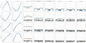
Here's an annotated version of the plot format I've been using previously. X axis is output current, first plot is gm, second is current gain, next are harmonics 2,3,4,5...

The turn-off spikes look like ringing is occurring, but that is a graphical artifact due to the way the test signal goes through the turn-off point: the 6kHz signal is not that small, so as it is swept through the problem spot, it hits it at a different part of its waveform depending on the offset. So the spikes occur in a different spot, and it displays the way it does.
Also... they are not really turn-off spikes as I measured with the scope earlier. They are picked up by the high gain current sense amplifier that measures the input current over a low value resistor, so I suspect they are simply magnetic coupling from the current in the transistor that turns off. That current loop is abruptly cut off when the transistor turns off, as current goes to flow in the other transistor instead. So the current quickly switches to another physical path. It's like in a DC-DC converter: optimizing the hot loop is the most crucial part of layout.
I think that's an interesting distortion mechanism. Self talked about magnetic coupling distortion due to class-B rectified currents radiating different magnetic fields because they take different paths. The board is 4 layer and the current paths run on top of each other to avoid it...... except through the emitter resistors, which make nice loop antennas standing above the pcb.
This distortion mechanism would also exist with a non-switching design, as that does not prevent the current from changing path from one transistor to the other at each crossover.
However, without emitter resistors, the crossover is much wider, so that "switching of current path" is much softer... and there are no emitter resistors to act as antennas. So the plot shows no spikes.
Anyway, back to non-switching...
With the FETs, nothing special happens when they turn off, also their turn-off is really soft due to low gm. The BJTs make spikes due to charge storage, but only when di/dt of the transistor that turns off exceeds a certain threshold. If it does not exceed that threshold, it just turns off without making a mess. It depends on the transistor, so I've ordered quite a few to investigate.
By removing the emitter resistors, class-A region is widened for the same bias current, so the transistor that will turn off does so at higher output current. Hopefully at this point di/dt is lower, but that depends on how angry the drummer is of course...
Removing the emitter resistors simply moves the threshold where spikes appear further away, but it doesn't solve the spike problem. That said, it's really effective: with 100mA bias current, turn-off occurs at about 800mA, and it is proportional to bias current, so at 200mA bias, you get +/-1.6A of class A. With reasonably efficient speakers... that's pretty safe.
What I don't like about the non-switching arrangements:
They try to emulate the gm of BJTs without resistors... so why not just use BJTs without resistors? It's faster, has better bandwidth, it's simple, and with the proper thermal compensation, it works. Will probably need cascode FET to avoid too much heating, which adds cost if the amp would only use one pair of MJL's, but is pretty much the same cost if the amp goes from 2xMJL pairs to one MJL pair and one IRFP cascode pair... because the cascodes help a lot with SOA. And there's no need to match parallel devices. So it's actually simpler. And two pairs of ThermalTraks are more expensive than one pair plus cascodes.
These non-switching designs seem very finicky... I've seen with CFPs that part-time feedback (ie the device that does the feedback turns off) is really a bad idea ; in most non-switching designs the feedback transistors don't turn off but their current (and transconductance, fT, etc) vary a lot so the open loop gain and phase of the internal feedback loop will move around, and it has to be stable over the whole range of parameters... smells like trouble...
Compared to an equivalent amount of feedback applied the usual way, they do not give better performance at lower bias, except for crossover spikes. So they have to be biased pretty high like 100mA anyway.
Besides practicality (no bias pot, no thermal sensor) which is nice, basically the only advantage would be to get rid of turn-off spikes, which would be cool with BJTs, but not really useful with FETs, because FETs don't make turn-off spikes. So a non-switching design with FETs is just basically a different, more finicky and difficult way to implement nested loop feedback... so why not just implement nested loop feedback instead?...
There is also this post
Basically if you run it at a bias current Ibias, and a current "Ialibi" is kept in the transistor that is prevented from turning off... then the dissipation corresponds to the total Ibias, but the useful bias that is actually used during the crossover to switch from one transistor to the other is Ibias - Ialibi, which means actual performance is identical to an output stage without resistors biased at Ibias - Ialibi.
So at equal bias, the switching design gets turn-off spikes, but the non-switching design gets worse static gm-dependent distortion, so it has to use more bias to catch up... no free lunch...
In a good AB design you can generally get H5, H7 and H9 at least lower than about 100dB, with even orders (H2 and H4) dominating the profile and a THD of about 0.01%.
Is it open loop or closed loop? At what output voltage/current/power?
Do you believe that if you can set up the outputs so that they never turn off you will improve significantly on these figures? This would improve the sound quality markedly if you could do it........
I'm not sure.
The algo measures THD not over the whole signal like a FFT does, instead it detects the harmonics of the 3-6 kHz tone at each point over the 40Hz period. So if there is misbehavior at turn-off, it appears on the plot at the output current point where it occurs, but the rest of the plot does not change at all.
It's a completely different way of measuring stuff. It's like doing a THD measurement while loading the output of the amp with a DC current source in addition to the load resistor, and stepping the value of the current source... If you did that experiment, and there was misbehavior at turn-off you'd expect an increase in THD when the DC current centers the AC test signal on the point where it happens. Except that wouldn't work, because DC would heat only one transistor and screw with the bias, which is why I'm using 40Hz and software.
Hmmm... It's difficult to explain without gestures and a whiteboard 😀
Suppose the output is loaded with a resistor, and the input signal is a sine with various values of DC added to it, as shown on the right. That DC will set the "center" point of the waveform somewhere on the wing diagram of the output stage.
So I plotted the THD residual of the output voltage, with gain and offset fudge factors to make the graph readable...
At the bottom of the graph, the DC sets the test signal in the gm-doubled portion of the wingspan where gm is pretty flat, so the THD residual is low. At the top, it is in the portion of the wingspan where one transistor conducts, so it is also pretty low. And in the middle, it is at the transition between gm-doubling and gm-not-doubling, so the THD resigual is much larger.
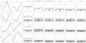
Here's an annotated version of the plot format I've been using previously. X axis is output current, first plot is gm, second is current gain, next are harmonics 2,3,4,5...
The turn-off spikes look like ringing is occurring, but that is a graphical artifact due to the way the test signal goes through the turn-off point: the 6kHz signal is not that small, so as it is swept through the problem spot, it hits it at a different part of its waveform depending on the offset. So the spikes occur in a different spot, and it displays the way it does.
Also... they are not really turn-off spikes as I measured with the scope earlier. They are picked up by the high gain current sense amplifier that measures the input current over a low value resistor, so I suspect they are simply magnetic coupling from the current in the transistor that turns off. That current loop is abruptly cut off when the transistor turns off, as current goes to flow in the other transistor instead. So the current quickly switches to another physical path. It's like in a DC-DC converter: optimizing the hot loop is the most crucial part of layout.
I think that's an interesting distortion mechanism. Self talked about magnetic coupling distortion due to class-B rectified currents radiating different magnetic fields because they take different paths. The board is 4 layer and the current paths run on top of each other to avoid it...... except through the emitter resistors, which make nice loop antennas standing above the pcb.
This distortion mechanism would also exist with a non-switching design, as that does not prevent the current from changing path from one transistor to the other at each crossover.
However, without emitter resistors, the crossover is much wider, so that "switching of current path" is much softer... and there are no emitter resistors to act as antennas. So the plot shows no spikes.
Anyway, back to non-switching...
With the FETs, nothing special happens when they turn off, also their turn-off is really soft due to low gm. The BJTs make spikes due to charge storage, but only when di/dt of the transistor that turns off exceeds a certain threshold. If it does not exceed that threshold, it just turns off without making a mess. It depends on the transistor, so I've ordered quite a few to investigate.
By removing the emitter resistors, class-A region is widened for the same bias current, so the transistor that will turn off does so at higher output current. Hopefully at this point di/dt is lower, but that depends on how angry the drummer is of course...
Removing the emitter resistors simply moves the threshold where spikes appear further away, but it doesn't solve the spike problem. That said, it's really effective: with 100mA bias current, turn-off occurs at about 800mA, and it is proportional to bias current, so at 200mA bias, you get +/-1.6A of class A. With reasonably efficient speakers... that's pretty safe.
What I don't like about the non-switching arrangements:
They try to emulate the gm of BJTs without resistors... so why not just use BJTs without resistors? It's faster, has better bandwidth, it's simple, and with the proper thermal compensation, it works. Will probably need cascode FET to avoid too much heating, which adds cost if the amp would only use one pair of MJL's, but is pretty much the same cost if the amp goes from 2xMJL pairs to one MJL pair and one IRFP cascode pair... because the cascodes help a lot with SOA. And there's no need to match parallel devices. So it's actually simpler. And two pairs of ThermalTraks are more expensive than one pair plus cascodes.
These non-switching designs seem very finicky... I've seen with CFPs that part-time feedback (ie the device that does the feedback turns off) is really a bad idea ; in most non-switching designs the feedback transistors don't turn off but their current (and transconductance, fT, etc) vary a lot so the open loop gain and phase of the internal feedback loop will move around, and it has to be stable over the whole range of parameters... smells like trouble...
Compared to an equivalent amount of feedback applied the usual way, they do not give better performance at lower bias, except for crossover spikes. So they have to be biased pretty high like 100mA anyway.
Besides practicality (no bias pot, no thermal sensor) which is nice, basically the only advantage would be to get rid of turn-off spikes, which would be cool with BJTs, but not really useful with FETs, because FETs don't make turn-off spikes. So a non-switching design with FETs is just basically a different, more finicky and difficult way to implement nested loop feedback... so why not just implement nested loop feedback instead?...
There is also this post
Basically if you run it at a bias current Ibias, and a current "Ialibi" is kept in the transistor that is prevented from turning off... then the dissipation corresponds to the total Ibias, but the useful bias that is actually used during the crossover to switch from one transistor to the other is Ibias - Ialibi, which means actual performance is identical to an output stage without resistors biased at Ibias - Ialibi.
So at equal bias, the switching design gets turn-off spikes, but the non-switching design gets worse static gm-dependent distortion, so it has to use more bias to catch up... no free lunch...
Because keeping a more or less constant phase relationship between the analog class A amplifier and the class D amplifier modulated power supplies (under all circumstances, clipping, etc...) is not trivial, in particular at high frequencies. It can be done, though, I've seen a few DIY implementations, but I have not seen any measurements, they all looked more or less like a proof of concept (which is obviously sound).
Bingo 😀
I've considered it, but it's a lot of work, EMI, etc. I did a few sims, quickly ditched the idea of using one class D amp and some floating supplies because what a mess, I would have used a 2 channel class D chip with integrated FETs from IR to generate both pos/neg floating supply.
But a class AB channel with 100mA bias and +/-40V rails will burn 8W, say 10-12W drivers included.
Idle dissipation of many class D amps that would suit such a design is not different from that. So would it save power? hmmm.... for a high power amp, maybe, but my speakers are reasonably efficient, so I don't need it...
ps: the PSRR sim in that post is wrong, because the two AC sources used for PSRR sim cancel each other.
Last edited:
I hope you can perform some testing with the SAnken pairs I've send you. I'm specifically tested when driven bij a Fet driver stage and 0R22 emitter resistors with 100mA Bias.
My amp has 7 pairs of SAnken with 1530/201 drivers biased at about 120mA. Would 1 pair of Sanken bjt's driven by Fet's biased at 120/7 = +-17mA be representative?
Thanks 😀
Yes, when modeling paralleled devices I increase the load resistor and decrease the current, that works.
I'm not sure about the drivers though. I should run the FETs at the same transconductance than yours to match, but I have no idea what that would be...
Anyway, here I am again with another Proton schematic I found, no emitter resistors, and 'modulated rails' (I don't know the correct terminology) for drivers and single pair outputs. Seems they were on to something similar back then too. However, it seems to have the same weak link with the bias as the one I mentioned before, and Iq probably set way too low from factory to keep it from smoking.
Yeah, higher Iq = higher gm = higher sensitivity of bias to Vbe tempco, so high bias really needs a thermal sensor that follows the temperature of the silicon...
I got the thermaltraks, I'll test the response of the built-in diode.
No offers from high-end manufacturers lol.
Last edited:
...and the comparison with the MOSFETs.
At 0R47 there was too much gm-doubling.
At 0R15 and 0R33, THD stopped getting lower around 260mA bias.
Without source resistors, the gm hole near zero current is too deep.
BJTs have high transconductance at reasonable bias currents, FETs need quite higher bias current to do the same.
So it looks like BJTs without emitter resistors win the prize, by offering lower distortion, both high and low order, at more reasonable bias current 😀
link to google drive with all the plots
Attachments
Hi peufeu,
That has been my experience over the years without doing the excellent, in depth work you have done. Now I know why that is.
You are on a roll with this. Time to explore driver configurations and other circuit configurations. You can take your best distortion position and try setting up roughly the same tests you have done before.
-Chris
Independent confirmation from experience, I like that 😀
It's been an interesting adventure!
So. The output topology is decided: BJTs without resistors, with optional MOSFET cascode.
However the board with the output stage on it looks like a war zone, covered in a thick crust of flux and some pads are lifting off.
It will do for testing a batch of various power BJT to see if there are better ones than the MJL's. So the plan is:
- Test ThermalTrak temperature sensor versus hack soldering a MMBT3904 on the collector lead. I expect ThermalTrak to win.
- Test a bunch of different BJTs for turn-off spikes and distortion, hFe droop, etc. I will do that when I have all the BJTs.
Then... the air-wired bias controller has died again. I need a new PCB to test the driver configurations, something more reliable, with proper plug-in modules this time. I also want to work on extending bandwidth with feedforward. And I have tons of other stuff to do in August. So it looks like there will be a month of hiatus, or as marketing says, "brainstorming"!

Please remind yourself that cascode bootstrapping includes a free variable, a designer-adjustable coefficient.
Cascode_drive_voltage(ac) = COEFFICIENT * input_signal(ac)
There's no absolute requirement that COEFFICIENT = (+1.0 - epsilon)
Cascode_drive_voltage(ac) = COEFFICIENT * input_signal(ac)
There's no absolute requirement that COEFFICIENT = (+1.0 - epsilon)
Yes, this is true, but I'm not sure it will be useful in this project: distortion due to nonlinear Cbc is proportional to 1-COEFFICIENT so I like it close to 1. But maybe it could be useful and I'm not seeing how. Suggestions?
Also, dissipating power in MOSFETs is cheaper than doing so in BJTs, so it makes sense to keep the BJT Vce low and have the cascode FET handle most of the heat.
Also, dissipating power in MOSFETs is cheaper than doing so in BJTs, so it makes sense to keep the BJT Vce low and have the cascode FET handle most of the heat.
Phenomenal series of posts full of informative experimental investigation; I've not seen or read the like anywhere.
Thank you!
Thank you!
So, I was thinking...
There is the turn-off spike that is due to transit time...
But there is also the crossover spike that is due to a different mechanism. Picture output current ramping up at constant di/dt ; the slopes of a sinewave are a good approximation. As this output current sweeps through the crossover, near the center there is a zone where gm is lower. So, feedback has to compensate by increasing the drive voltage slew rate.
That's the voltage between input and output of an EF output stage. In the crossover zone near zero there is an increase in slope because there is a decrease in transconductance:

Through the low gm zone, to output the required di/dt current slew rate, the thing must be driven harder, with higher voltage slew rate (dv/dt). Since the input capacitance is quite large, this increase in dv/dt at the input due to lower gm creates a spike in the input current. This does not happen at turn-off, but in the center of the crossover where gm drops.
I've added the THD residual of input current on top: the two spikes show up.

These are small but they contain a lot of high frequency energy for their size, for example the downward slope of the small spike lasts about 500ns... and that's what caused MJE15030/15031 to make a big mess, because at the rather low driver idle current, their fT is too low, just a few MHz, so if something happens in 500ns, they won't do anything useful like provide current gain. Instead they will just pass the hot potato through their B-E capacitance to the predrivers, let'em deal with that.
So the predrivers see the low frequency components of the OPS base current divided by driver hFe (as expected) but this does not apply to the high frequency components. So that spike is 2mA tall, which seems tiny, but if it goes straight to the predrivers, for them it's a huge signal. If the output stage has a current gain of 10k, which is realistic with hFe 100 drivers and outputs, the predrivers would expect to output 2mA if actual output current was 20A, to give an idea of the scale of this stuff. And if the predrivers also have low fT at their idle current...

On the other hand, drivers with high fT at the idle current they're actually being used at in the circuit will do their job and provide the expected current gain. For example C5706/A2039 keep fT 100MHz at 10mA, so predrivers will see the same spike, but divided by driver current gain, in this case about 100.
Anyway. Since both these annoyances are proportional to di/dt, I thought, while hauling some drywall for renovation...
Why not boost the bias in proportion to di/dt?
It is not a non-switching design. It's a non-spiking output stage.
We already have a lossless sensor that computes di/dt, it's the output inductor. Measure voltage on it, apply some math fudge like log(smoothed absolute value) and add to bias voltage. With in green, without in red. This is a sim, there is no actual (nor virtual) circuit doing the thing, I just added the math in the function voltage source.

Results are interesting: All the HF crossover spikes disappear. High harmonics drop a lot quicker. Basically it boosts the bias to 650mA only during the time window where it is needed, and after that it goes back to normal.
Both the defect (spikes) and the correction circuit are proportional to di/dt, which is proportional to product of frequency and amplitude. Which means on low frequency signals, it does nothing... which is fine, because there is also no defect to correct.
There is the turn-off spike that is due to transit time...
But there is also the crossover spike that is due to a different mechanism. Picture output current ramping up at constant di/dt ; the slopes of a sinewave are a good approximation. As this output current sweeps through the crossover, near the center there is a zone where gm is lower. So, feedback has to compensate by increasing the drive voltage slew rate.
That's the voltage between input and output of an EF output stage. In the crossover zone near zero there is an increase in slope because there is a decrease in transconductance:
Through the low gm zone, to output the required di/dt current slew rate, the thing must be driven harder, with higher voltage slew rate (dv/dt). Since the input capacitance is quite large, this increase in dv/dt at the input due to lower gm creates a spike in the input current. This does not happen at turn-off, but in the center of the crossover where gm drops.
I've added the THD residual of input current on top: the two spikes show up.
These are small but they contain a lot of high frequency energy for their size, for example the downward slope of the small spike lasts about 500ns... and that's what caused MJE15030/15031 to make a big mess, because at the rather low driver idle current, their fT is too low, just a few MHz, so if something happens in 500ns, they won't do anything useful like provide current gain. Instead they will just pass the hot potato through their B-E capacitance to the predrivers, let'em deal with that.
So the predrivers see the low frequency components of the OPS base current divided by driver hFe (as expected) but this does not apply to the high frequency components. So that spike is 2mA tall, which seems tiny, but if it goes straight to the predrivers, for them it's a huge signal. If the output stage has a current gain of 10k, which is realistic with hFe 100 drivers and outputs, the predrivers would expect to output 2mA if actual output current was 20A, to give an idea of the scale of this stuff. And if the predrivers also have low fT at their idle current...
On the other hand, drivers with high fT at the idle current they're actually being used at in the circuit will do their job and provide the expected current gain. For example C5706/A2039 keep fT 100MHz at 10mA, so predrivers will see the same spike, but divided by driver current gain, in this case about 100.
Anyway. Since both these annoyances are proportional to di/dt, I thought, while hauling some drywall for renovation...
Why not boost the bias in proportion to di/dt?
It is not a non-switching design. It's a non-spiking output stage.
We already have a lossless sensor that computes di/dt, it's the output inductor. Measure voltage on it, apply some math fudge like log(smoothed absolute value) and add to bias voltage. With in green, without in red. This is a sim, there is no actual (nor virtual) circuit doing the thing, I just added the math in the function voltage source.
Results are interesting: All the HF crossover spikes disappear. High harmonics drop a lot quicker. Basically it boosts the bias to 650mA only during the time window where it is needed, and after that it goes back to normal.
Both the defect (spikes) and the correction circuit are proportional to di/dt, which is proportional to product of frequency and amplitude. Which means on low frequency signals, it does nothing... which is fine, because there is also no defect to correct.
Last edited:
Here's a design I wanted to try, I think it's called "hyperbolic class A" or something. I've seen several variants on the forum.

This design was patented in 1984, which is good news, since the patent has since expired. This is not the Devialet patent which uses part-time feedback and therefore sucks.
The idea is to replace emitter resistors with schottky diodes, and impose a constant voltage across these diodes by means of the two control transistors at the input. This creates an exponential ("hyperbolic") crossover, just like BJTs without resistors.
There is a convenient spot for a compensation capacitor (two, in fact). I had no stability issues with this implementation:

If that works, it probably means it's not a temperamental circuit...
In the schematic, I21 and I22 are CCS that add a bit of voltage over the 470R resistors to compensate for the difference between Q52-Q53 Vbe and lower Schottky diode Vf. In this implementation these CCS turn on Q52-Q53 enough so the output stage bias current is zero. Then, I20, which is an optocoupler disguised as a current source and controlled by the micro, sinks some of the current from the CCS to turn on Q52-Q53 less, which allows the voltage between Q1/Q2 bases to rise, and sets the bias. This means bias is zero until the micro sets it, which is convenient for not smoking stuff at power-up. I20 can also be replaced by a pot for manual adjustment.
I've seen variations with other Schottky diodes to compensate the Vf of the big ones, control transistors thermally coupled to the diodes or not, etc. I didn't bother.
Of note, this has three possible input nodes: the point between the emitters of both control transistors (used as input in schematic) and the collectors of Q52-Q53 for a more classical use case with a VAS. In this latter case, the Cdom compensation cap could be connected to one of the collectors, or to the emitters, so that makes even more combinations.
Power transistors could also be MOSFETs.
This design was patented in 1984, which is good news, since the patent has since expired. This is not the Devialet patent which uses part-time feedback and therefore sucks.
The idea is to replace emitter resistors with schottky diodes, and impose a constant voltage across these diodes by means of the two control transistors at the input. This creates an exponential ("hyperbolic") crossover, just like BJTs without resistors.
There is a convenient spot for a compensation capacitor (two, in fact). I had no stability issues with this implementation:
If that works, it probably means it's not a temperamental circuit...
In the schematic, I21 and I22 are CCS that add a bit of voltage over the 470R resistors to compensate for the difference between Q52-Q53 Vbe and lower Schottky diode Vf. In this implementation these CCS turn on Q52-Q53 enough so the output stage bias current is zero. Then, I20, which is an optocoupler disguised as a current source and controlled by the micro, sinks some of the current from the CCS to turn on Q52-Q53 less, which allows the voltage between Q1/Q2 bases to rise, and sets the bias. This means bias is zero until the micro sets it, which is convenient for not smoking stuff at power-up. I20 can also be replaced by a pot for manual adjustment.
I've seen variations with other Schottky diodes to compensate the Vf of the big ones, control transistors thermally coupled to the diodes or not, etc. I didn't bother.
Of note, this has three possible input nodes: the point between the emitters of both control transistors (used as input in schematic) and the collectors of Q52-Q53 for a more classical use case with a VAS. In this latter case, the Cdom compensation cap could be connected to one of the collectors, or to the emitters, so that makes even more combinations.
Power transistors could also be MOSFETs.
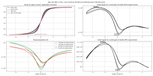
It behaves very much like the resistor-free output stage, but with some differences. First two plots are this "hyperbolic" OPS, last 2 plots are resistor-free cascoded MJLs.
The first interesting result is that the crossover zone is absolutely huge. With "200mA" bias, turn-off occurs at around 2.5A output current. At 100mA, turn-off seems to occur at around 1.5A which is the same as the plain resistor-free OPS at 200mA. So it gives even more class A for the same price in terms of wasted idle power.
I believe this is due to the diodes having lower internal resistance than the BJT emitters, perhaps from shorter bondwires or something. So it is even more "resistor-free" than the resistor-free OPS 😀 but it could also be due to different I-V characteristics.
This wider crossover means the transition between hFe's of the top and bottom halves of the OPS is smoother, which is good.
Bias did increase due to self heating, so it is about 50% higher than what the plot says. This tempers the "more class A from the same price" result but not completely.
Vf across the diodes is tiny, but their thermal mass is much lower than MJL3281, which means some self-heating occurs. This is visible in the "doubling" of the plots. These plots are all loops, from one period of the signal, so if it gets hot and bias current increases on the way up, then it will follow a different path on the way down. But... without resistors, there is no gm-doubling, so the only thing a transient increase in bias actually does is lower distortion. Bias increase due to diode self-heating is transient and it goes back to normal as soon as they cool. So this could actually be a feature.
Anyway, the diodes would probably need to be thermally coupled to the control transistors, for example screwed on both sides of a PCB heat sink.
Attachments
-
 gm-Bias 200.000 m, PSU +10.0-10.0V,AC 64.000 mA 6.000 kHz,load 7.6R,HFin,LFout-MJL1302-3281 v14 .png266.6 KB · Views: 414
 -
 gm-Bias 100.000 m, PSU +10.0-10.0V,AC 64.000 mA 6.000 kHz,load 7.6R,HFin,LFout-MJL1302-3281 v14 .png237.3 KB · Views: 446
 -
 gm-Bias 100.000 m, PSU +20.0-20.0V,AC 64.000 mA 6.000 kHz,load 7.6R,HFin,LFout-MJL1302-3281 v13 .png170.6 KB · Views: 427
 -
 gm-Bias 200.000 m, PSU +20.0-20.0V,AC 64.000 mA 6.000 kHz,load 7.6R,HFin,LFout-MJL1302-3281 v13 .png187.6 KB · Views: 431
Last edited:
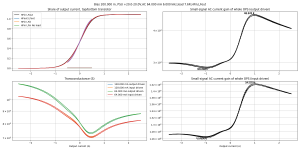
Now, distortion...
This time the resistor-free BJTs are on the left (100mA and 200mA bias) ; and the "hyperbolic diodes" on the right.
Distortion is even lower! Especially near zero current where it matters most. The transient bias increase "feature" most likely plays a part here.
In other words, this output stage topology is scoring a lot of points here.
I simulated it with FETs: distortion increased. This is most likely because the amount of feedback available is low, but with BJTs the correction that is applied by the control transistors is quite small too, since we're using BJTs to emulate the crossover of an ideal BJT output stage. They're already most of the way there. On the other hand MOSFETs need a much larger amount of correction to stop behaving like MOSFETs and emulate BJTs instead. So, no surprises.
I did another round of simulations, this time changing the input node from the emitters of the control transistors to the collectors. This adds the Vbe (or Vgs) of one output transistor to the output voltage, so it is worse. With BJTs there was not much change, but with FETs there was a substantial increase in distortion, because Vgs swings are much larger.
Attachments
-
 thd-Bias 100.000 m, PSU +20.0-20.0V,AC 64.000 mA 3.000 kHz,load 7.6R,HFin,LFout-MJL1302-3281 v13.jpg775.8 KB · Views: 408
 -
 thd-Bias 200.000 m, PSU +20.0-20.0V,AC 64.000 mA 3.000 kHz,load 7.6R,HFin,LFout-MJL1302-3281 v13.jpg753.5 KB · Views: 166
 -
 thd-Bias 100.000 m, PSU +10.0-10.0V,AC 64.000 mA 3.000 kHz,load 7.6R,HFin,LFout-MJL1302-3281 v14.jpg784.9 KB · Views: 145
 -
 thd-Bias 200.000 m, PSU +10.0-10.0V,AC 64.000 mA 3.000 kHz,load 7.6R,HFin,LFout-MJL1302-3281 v14.jpg780.3 KB · Views: 144
So this output stage behaves best when driven through the emitters of the control transistors.
It is also possible to add another pair of control transistors whose base is referenced to the output, like in the design Elvee posted earlier, to make a low cost nested feedback loop.
Thermal compensation is much simpler than for a resistor-free BJT output stage, because the diodes don't dissipate much, so they only need a small heat sink, and the sensor transistor (which is also the control transistor) can be simply screwed on the back of this heat sink right behind the diode. Also the component whose "Vbe" determines the bias now is the diode, and dissipates much less little power than the transistor because its Vf is tiny, which means there is less risk of runaway.
Todolist for tomorrow:
- Add a resistor between the emitters of the power transistors to make it non-switching (the diodes will still switch)
- Measure performance with the input on one collector instead of on the emitters as it is now
- Frequency response test and crossover spike test
i think SAE did something like this many years ago.
i never knew it was patented!
i think they called it hyper-something, maybe theirs was called "Hypersonic Class-A".
Big schottkys in place of or in parallel with emitter resistors on the output BJTs .
time to check the wayback machine ....
BTW peufeu, i echo the sentiments of others that you're doing a great job! this is extremely interesting and very useful information.
Here's a design I wanted to try, I think it's called "hyperbolic class A" or something. I've seen several variants on the forum.
...
Thanks!
I've looked into it a bit, and found this "HYPERSONIC CLASS A" (lmao) in SAE X-25 amp, but...

it's not the same, they just put diodes in series with the emitter resistors without the circuit that keeps voltage constant across them... That softens the crossover a bit, but it halves the transconductance of the BJTs, so according to Spice it needs at least 500mA bias to get similar gm to the hyperbolic circuit at 100mA, quite impractical.
I've tried driving the hyperbolic circuit from the collector of the top transistor. Result is a very slight increase in H2 (a few dB) that doesn't seem significant.
I've looked into it a bit, and found this "HYPERSONIC CLASS A" (lmao) in SAE X-25 amp, but...
it's not the same, they just put diodes in series with the emitter resistors without the circuit that keeps voltage constant across them... That softens the crossover a bit, but it halves the transconductance of the BJTs, so according to Spice it needs at least 500mA bias to get similar gm to the hyperbolic circuit at 100mA, quite impractical.
I've tried driving the hyperbolic circuit from the collector of the top transistor. Result is a very slight increase in H2 (a few dB) that doesn't seem significant.
Great work, peufeu! This is a very interesting Thread.
I may have missed it, did you also measurements with a complex load (loudspeaker)?
I may have missed it, did you also measurements with a complex load (loudspeaker)?
Thanks!
I didn't use a complex load. This setup measures distortion due to output current which is shown on the X axis of all the plots. If current is out of phase with voltage, then this distortion will occur on a different place on the voltage waveform, but it will always occur on the same place on the current waveform, because crossover is always centered on zero current.
Looking at it from a voltage perspective, making current out of phase with voltage would move current-related distortion (non-flat gm, etc) to a different place in the cycle, but voltage-related distortion (nonlinear capacitance, Early effect, etc) would stay in the same place. Same thing if you look at it from a current perspective, just swap "voltage" and "current" in the previous sentence.
So if voltage-related distortion was significant then both could add in different ways... but it is not, the last row of the plot (without load) shows it is tiny compared to current-related distortion. I included it to make sure voltage-related distortion did not cancel out some current-related distortion, because that would spoil the measurement.
- Home
- Amplifiers
- Solid State
- Power amp OUTPUT STAGE measurements shootout