I concentrate on the main mechanism only, not on the performances which are different.Current flows out of the inverting input on a CFA - and the magnitude depends on the compensation capacitor value and frequency and that's why using a square wave stimulus will show the differences in operation that you will not see at DC.
Absolutely. I underlined the feature that was not yet much emphasized, thanks for having reminded it. Since long, my approach is to observ the load of the inverting input emitter.In a CFA you develop a voltage across Rg from the current injected into it from the buffer emitter and Rf driven from the output stage.
It was not exactly my purpose.VFA's don't work like that so I don't know how you can make your claim that they are the same i.e. voltage feedback amplifiers.
I watched the input transistor of a CFA (one transistor only), of a BFA (ideally buffered feedback network) and of a VFA (differential input = realistically buffured feedback network).
I noticed that, using identical DC conditions, it shows almost the same Vbe voltage and Ie current in the three scenarios (the various capacitances of the whole circuit are neglected, of course).
For me, the fundamental mechanism of feedback amplifiers, CFA or VFA, relies in this transistor.
Last edited:
For my own amusement, i have been interested in low to moderate OLG circuits which are inherently linear as a starting point for audio.
I have never had any trouble getting ppm levels of distortion. Even levels into the -140's dBv withOut high OLG. But you do have to have very good complimentary transistors. Which is becoming No easy task. However, with new IC processes being able to make true compliments, it should not be an issue any more.
Power amps for driving speakers is still a challenge as they still rely on mostly discrete parts. Would a power amp of 200W/8 using inherently linear topologies derived from CMA and having the highest slew rate, lowest distortion, widest BW, unchanging over any freq and any load Z and output level sound the best/most accurate?
IMHO, of course, the answer is Yes.")
THx-RNMarsh
I have never had any trouble getting ppm levels of distortion. Even levels into the -140's dBv withOut high OLG. But you do have to have very good complimentary transistors. Which is becoming No easy task. However, with new IC processes being able to make true compliments, it should not be an issue any more.
Power amps for driving speakers is still a challenge as they still rely on mostly discrete parts. Would a power amp of 200W/8 using inherently linear topologies derived from CMA and having the highest slew rate, lowest distortion, widest BW, unchanging over any freq and any load Z and output level sound the best/most accurate?
IMHO, of course, the answer is Yes.
THx-RNMarsh
Last edited:
However, with new IC processes being able to make true compliments, it should not be an issue any more.
They can't, pesky holes vs. electrons.
Fully agreed when you would say, no return current.Withouta loop, no return voltage
Here I do also agree, without Rf no return current can flow and you can’t run a DIT.without a return voltage, no loop gain calculations; without loop gain calculations, you can't do Middlebrook's test.
You can however come close to open-loop when applying a very large resistor Rf like 10.000 times Rg.
That’s what I did in the Sim I made for Ian.
It returned in that case still enough information to classify the circuit as a CFA.
But, in hindsight, it was a silly one off experiment that doesn’t look to be very useful for whatever purpose. So let's forget this one.
That procedure could be by using the circuit below, being really an open-loop, like mentioned in #1391.If there is some procedure that you propose for the open loop case, please state it.
Dividing V(out)/(V(in+)-V(in-)) returns the open-loop gain.
And I would like to repeat, this uniquely separates the CFA from the VFA because it only applies to a CFA.
Hans
Attachments
I tried a "classical" long tail VFA versus this one based on CFA topology.Thanks for the effort, that was the idea. I was hoping to show that an equivalent CFA does not do significantly better when both are optimized for an audio application, though typically the CFA will have more noise. BTW I suspect LTspice is overly optimistic vs. something actually built on a PC board so this might not as useful as it could. Every little circuit I tried can get down to ppm levels.
The classical version produced more than 10 times as much IMD.
I didn't yet measure the noise produced, but that's simply done, I'll come back on that.
Hans
I concentrate on the main mechanism only, not on the performances which are different.
Absolutely. I underlined the feature that was not yet much emphasized, thanks for having reminded it. Since long, my approach is to observ the load of the inverting input emitter.
It was not exactly my purpose.
I watched the input transistor of a CFA (one transistor only), of a BFA (ideally buffered feedback network) and of a VFA (differential input = realistically buffured feedback network).
I noticed that, using identical DC conditions, it shows almost the same Vbe voltage and Ie current in the three scenarios (the various capacitances of the whole circuit are neglected, of course).
For me, the fundamental mechanism of feedback amplifiers, CFA or VFA, relies in this transistor.
You are just on a completely wrong track forr. We will have to leave it at that.
It has been said a lot of times. But nobody told me that my simulations are wrong. They do not need me to speak.You are just on a completely wrong track forr.
Scott,
can you live with this.
10mA current supply,
Pot are the two resistors R2 and R3, together 20k.
Gain is 20dB.
Load 600 Ohm.
Hans
Hi I'm looking at the circuit you have put up, it looks like an inverting VFA where R2 and R3 are the feedback resistors setting the 20 dB gain. R2 and R3 isn't a volume pot as you say.
I thought Scott was interested in a 10k source R.
Another thing where have you put the compensation C?
If you have gotten rid of the standard THD rise at 6kHz (or so) and dare to present wide(er) band measurements without the standard HF filter - and it still looks OK - please step forward! The world needs you!
//
Tjenare TNT
The THD vs frequency is more or less flat.
I thought Scott was interested in a 10k source R.
Not to be too rigorous, just some realistic source resistance as if the volume control is at the input of the line stage. The gain structure issue is worth talking about separately, I see no reason to have a level control at more than one point in a well thought out signal chain. Another discussion might be why should a volume control go from absolute silence to 10dB over hard clipping? This is a real problem, every month or so someone with very high sensitivity speakers can't get one of the popular DSP boards to work without excess noise/distortion i.e. they are using only the 14 or so LSB's.
Last edited:
You can however come close to open-loop when applying a very large resistor Rf like 10.000 times Rg.
Hans, you may already know this, but there is an undocumented feature in LTspice that lets you specify a separate value for DC analysis and AC analysis for a resistor. So you can do an operating point with a 'reasonable' resistance value, and then use 10Gigohm for the AC which should be like open loop.
Dual Value Resistors (for ac analysis)
LTspice is like Hspice in that it allows resistors to have different dc and ac values. If ac=<value> is specified as a resistor parameter (either immediately after the normal dc value or in the Value2 field), the operating point is calculated using the dc value of resistance, but the ac resistance value is used in the ac analysis. This may be useful when analyzing operational amplifiers, since the operating point computation can be performed on the unity gain configuration using a low value for the feedback resistance and the ac analysis may then be performed on a nearly open loop configuration by specifying a very large value for the ac resistance.
From: Undocumented LTspice - LTwiki-Wiki for LTspice
Jan
Last edited:
Fully agreed when you would say, no return current...
Ahhh, yes! We are in agreement. However, what good is measuring the voltage loop gain without the current loop gain? Some thoughts...
For VFA voltage gains:
Michael Steffes breaks the loop and places a 1 GigaHenry inductor in series and a 1 GigaFarad Capacitor in shunt. A voltage source can be inserted between the capacitor and ground to get the open loop voltage gain.
For current gains:
Connect the output of the D.U.T. to ground through a 1GigaFarad (1GF) capacitor. The input current source goes to the (-) input with the (+) input grounded. In addition, for a VFA, connect a 1 GigaHenry (1GH) inductor between the output and inverting input.
The problem here is that the different places of the capacitor in the two circuits violates the Middlebrookian requirement that the return analysis be performed at the same point in the same circuit. I'm skeptical that something like this technique will help us determine the predominant form of feedback.
This was Scotts cryptic brief.Hi I'm looking at the circuit you have put up, it looks like an inverting VFA where R2 and R3 are the feedback resistors setting the 20 dB gain. R2 and R3 isn't a volume pot as you say.
I thought Scott was interested in a 10k source R.
Another thing where have you put the compensation C?
Question for all, take 15V rails, your choice of resistors and capacitors, and nothing but say 3904's and 3906's.
To be somewhat arbitrary pick a useful task like a non-inverting 20dB line stage driving 600 Ohms from a 20K volume control and make the metric the distortion floor of a standard multi-tone signal at 2V rms.
I used a 20K pot like in the brief but an inverting VFA.
R2 and R3 are for certain the volume pot.
Look elsewhere in this forum for the Bruno Putzeys Balanced Preamp, or BPBP for short.
The two parts of the pot are setting the gain.
But as Scott warns, there should be a stop in whatever form to prevent the gain from exceeding a certain value. But you can find all about this in the BPBP thread.
Last but not least, there is no compensation C. It is not a classic VFA with a Miller cap, the topology is based om a CFA.
Hans
Hi Chris,Ahhh, yes! We are in agreement. However, what good is measuring the voltage loop gain without the current loop gain? Some thoughts...
For VFA voltage gains:
Michael Steffes breaks the loop and places a 1 GigaHenry inductor in series and a 1 GigaFarad Capacitor in shunt. A voltage source can be inserted between the capacitor and ground to get the open loop voltage gain.
For current gains:
Connect the output of the D.U.T. to ground through a 1GigaFarad (1GF) capacitor. The input current source goes to the (-) input with the (+) input grounded. In addition, for a VFA, connect a 1 GigaHenry (1GH) inductor between the output and inverting input.
The problem here is that the different places of the capacitor in the two circuits violates the Middlebrookian requirement that the return analysis be performed at the same point in the same circuit. I'm skeptical that something like this technique will help us determine the predominant form of feedback.
I will read this carefully and come back to you.
Hans
Jan,Hans, you may already know this, but there is an undocumented feature in LTspice that lets you specify a separate value for DC analysis and AC analysis for a resistor. So you can do an operating point with a 'reasonable' resistance value, and then use 10Gigohm for the AC which should be like open loop.
Dual Value Resistors (for ac analysis)
LTspice is like Hspice in that it allows resistors to have different dc and ac values. If ac=<value> is specified as a resistor parameter (either immediately after the normal dc value or in the Value2 field), the operating point is calculated using the dc value of resistance, but the ac resistance value is used in the ac analysis. This may be useful when analyzing operational amplifiers, since the operating point computation can be performed on the unity gain configuration using a low value for the feedback resistance and the ac analysis may then be performed on a nearly open loop configuration by specifying a very large value for the ac resistance.
From: Undocumented LTspice - LTwiki-Wiki for LTspice
Jan
Thanks for making me aware of this and no, I didn't know.
Hans
It has been said a lot of times. But nobody told me that my simulations are wrong. They do not need me to speak.
No one argues with your simulations, forr, but rather your interpretations of them. To brutalize (pun intended) Shakespeare:
"The fault, dear forr, is not in our stars, but in ourselves."
In my simulated circuits (links below), I showed that, for the same working conditions, the AC current Ie and the AC Vbe of T1 are independant of the resistor values of the feedback network up to 10 kOhm. This remains true even if a buffer or an emitter follower is inserted between the midpoint of the network and the emitter of T1. It a fundamental fact you can't deny. It is up to everybody to interpret as he wantsNo one argues with your simulations, forr, but rather your interpretations of them.
I have the strange feeling that my work displeases.
post #1307
Current Feedback Amplifiers, not only a semantic problem?
post #1396
Current Feedback Amplifiers, not only a semantic problem?
In my simulated circuits (links below), I showed that, for the same working conditions, the AC current Ie and the AC Vbe of T1 are independant of the resistor values of the feedback network up to 10 kOhm. This remains true even if a buffer or an emitter follower is inserted between the midpoint of the network and the emitter of T1. It a fundamental fact you can't deny. It is up to everybody to interpret as he wants
I have the strange feeling that my work displeases.
It is your selective recitation of facts and refusal to consider or even respond to others that cements your intransigence.
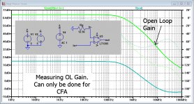
Thanks for following through on my query in Post 1321 for Rf very large or the case of no Rf.That procedure could be by using the circuit below, being really an open-loop, like mentioned in #1391.
Dividing V(out)/(V(in+)-V(in-)) returns the open-loop gain.
And I would like to repeat, this uniquely separates the CFA from the VFA because it only applies to a CFA.
But doesn't your open loop test bring an apparent contradiction with it? How can you say you have a CFA when there is no feedback in open loop? Wouldn't it then be just a CA
? Or could it be that even in open loop it is still a CFA with current feedback active?
I suggested that there is still current feedback in open loop as emitter degeneration of the input stage. Your voltage gain plots show about 48dB difference between them and assuming this is due to degeneration feedback in the input stage then we can calculate the Rn or 1/gm as 12k5/250 (from 48dB) or Rn~50 ohms and is in the right ball-park of 25-50 ohms. That supports the idea that the 12k5 gives 48dB of degenerative feedback to the input stage in this open loop test.
Then, if Rf is reintroduced, you get current fed into the emitter resistor that relieves the input transistor of current since there is a lot of current gain in the output buffer (~10,000 times). Reducing Rf to a small value (say Rg or less) then most of the feedback current into the emitter resistor comes from the output buffer with only 1/10,000th of the current needed from the input transistor. This can explain current feedback in a CFA at DC and LF..
But what about VFA's including H-bridge or buffered CFA's (which are VFA's)?
I think the Middlebrook/Franco observation that you have a CFA when there is enough degeneration of the input stage with a tipping point at 3dB of degenerative current feedback in the input stage, and then a factor of 10 (or 20dB) to be clear of the transition region where we have a mix of both.
That might sound like a useful method for classification but the DIT test (Post 1335 -thanks Hans) did not show up the 20dB of degeneration in the LT1364 with 500 ohms of emitter degeneration, which using my 20dB degeneration test would classify it as a CFA contrary to the datasheets classification.
- Home
- Amplifiers
- Solid State
- Current Feedback Amplifiers, not only a semantic problem?