Question to Guru Wurcer. In his paper linked to earlier, Ramus says this:
"Comparing Voltage and Current Feedback Op Amps: Two parts on the same process, at the same quiescent power, will have pretty similar open loop gain curves for VFB and CFB devices – Compare the OPA690 (VFB) and the OPA691 (CFB) below"
Why would he say that? Does a given process and power budget ultimately limit the attainable bandwidth/gain from a device?
Jan
Good paper, thanks Jan!
Backs up everything I've been saying, notable on page 31: "For Current Feedback op amps, the loop gain is set by the feedback impedance allowing an independent setting for the signal gain" (underline mine).
As a helper construct for our understandning I like to use the Thevenin equivalent of the standard feedback network which presents a fraction Rg/(Rf+Rg) of the output voltage via a series impedance of Rf//Rg=Rf*Rg/(Rf+Rg).
If we introduce a factor a=Rg/Rf ==> Rg=a*Rf we get:
Feedback Voltage Factor ß : a*Rf/(Rf+a*Rf) = a/(1+a),
Feedback Impedance I : a*Rf²/(Rf + a*Rf) = Rf * a/(1+a).
In a CFA OLG goes with 1/I (AOL curve shifted upwards) within resonable limits, and noise gain is 1/ß as ususal (thus, 1/ß curve shifted upwards by the same amount).
This perfectly explains the self-compensating bandwith property of the standard divider with Rg varied for gain and Rf held constant. Without that simple model, many people (and this comprises not only newcomers) have difficulties to understand -- or at least, to express -- how a CFA maintains constant BW vs. gain in the standard circuit. When I was first introduced to CFAs I've asked seasoned professionals and they came up with pretty complex stuff instead of using this simple and straightforward explanation which I also seldom find presented explicitly in text books, that's why I keep riding that horse : the gain-bandwith independance isn't a feature of the CFA itself, it a feature of a CFA *when used* with a very specific feedback network ;-)
Last edited:
If this is meaningless, the feedback current can't be claimed to be distinct from voltage feedack in a CFA.FORR Is it the feedback current which determines Vbe or Vbe which determines the feedback current ?
This is as meaningless a question as asking whether a current through a resistor causes a voltage across it or a voltage across it causes a current through it.
A voltage source causes a current across a resistor
A current source causes a voltage at the ends of a resistor.
The currrent in current feedback does not emanate from a current source, it can't "force" the Vbe like it is the case in the common base transistor of a cascode.
The input current is controlled by Vbe otherwise the circuit is not under control.
Question to Guru Wurcer. In his paper linked to earlier, Ramus says this:
"Comparing Voltage and Current Feedback Op Amps: Two parts on the same process, at the same quiescent power, will have pretty similar open loop gain curves for VFB and CFB devices – Compare the OPA690 (VFB) and the OPA691 (CFB) below"
Why would he say that? Does a given process and power budget ultimately limit the attainable bandwidth/gain from a device?
Jan
Jan
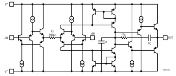
From the OPA690 datasheet:
"Typical differential input stages used for voltage feedback op amps are designed to steer a fixed-bias current to the compensation capacitor, setting a limit to the achievable slew rate. The OPA690 uses a new input stage which places the transconductance element between two input buffers, using their output currents as the forward signal."
In other words I guess its a H-Bridge inputstage.😉
Cheers
Good paper, thanks Jan!
Backs up everything I've been saying, notable on page 31: "For Current Feedback op amps, the loop gain is set by the feedback impedance allowing an independent setting for the signal gain" (underline mine).
As a helper construct for our understandning I like to use the Thevenin equivalent of the standard feedback network which presents a fraction Rg/(Rf+Rg) of the output voltage via a series impedance of Rf//Rg=Rf*Rg/(Rf+Rg).
If we introduce a factor a=Rg/Rf ==> Rg=a*Rf we get:
Feedback Voltage Factor ß : a*Rf/(Rf+a*Rf) = a/(1+a),
Feedback Impedance I : a*Rf²/(Rf + a*Rf) = Rf * a/(1+a).
In a CFA OLG goes with 1/I (AOL curve shifted upwards) within resonable limits, and noise gain is 1/ß as ususal (thus, 1/ß curve shifted upwards by the same amount).
This perfectly explains the self-compensating bandwith property of the standard divider with Rg varied for gain and Rf held constant. Without that simple model, many people (and this comprises not only newcomers) have difficulties to understand -- or at least, to express -- how a CFA maintains constant BW vs. gain in the standard circuit. When I was first introduced to CFAs I've asked seasoned professionals and they came up with pretty complex stuff instead of using this simple and straightforward explanation which I also seldom find presented explicitly in text books, that's why I keep riding that horse : the gain-bandwith independance isn't a feature of the CFA itself, it a feature of a CFA *when used* with a very specific feedback network ;-)
I like this - very simple explanation for CFA gain-bandwidth independence.
Good paper, thanks Jan!
Backs up everything I've been saying, notable on page 31: "For Current Feedback op amps, the loop gain is set by the feedback impedance allowing an independent setting for the signal gain" (underline mine).
As a helper construct for our understandning I like to use the Thevenin equivalent of the standard feedback network which presents a fraction Rg/(Rf+Rg) of the output voltage via a series impedance of Rf//Rg=Rf*Rg/(Rf+Rg).
If we introduce a factor a=Rg/Rf ==> Rg=a*Rf we get:
Feedback Voltage Factor ß : a*Rf/(Rf+a*Rf) = a/(1+a),
Feedback Impedance I : a*Rf²/(Rf + a*Rf) = Rf * a/(1+a).
In a CFA OLG goes with 1/I (AOL curve shifted upwards) within resonable limits, and noise gain is 1/ß as ususal (thus, 1/ß curve shifted upwards by the same amount).
This perfectly explains the self-compensating bandwith property of the standard divider with Rg varied for gain and Rf held constant. Without that simple model, many people (and this comprises not only newcomers) have difficulties to understand -- or at least, to express -- how a CFA maintains constant BW vs. gain in the standard circuit. When I was first introduced to CFAs I've asked seasoned professionals and they came up with pretty complex stuff instead of using this simple and straightforward explanation which I also seldom find presented explicitly in text books, that's why I keep riding that horse : the gain-bandwith independance isn't a feature of the CFA itself, it a feature of a CFA *when used* with a very specific feedback network ;-)
Almost. I speak of the constant bandwidth requirement in Current Feedback: Fake News or the Real Deal? | audioXpress. It is to a good approximation that Zin (inverting input stage) < Rg || Rf , holding Rf constant and varying Rg. And if you were foolish enough to drive a VFA this way, you'd see that too.
What you would not see in a VFA is the slew rate enhancement on demand effect of a CFA. In a classical VFA, the input stage bias current creates an upper limit for slewing the compensation capacitor voltage. But in a CFA, the input stage can get significant additional help from the current flowing into it from the outside.
So in a CFA, it is ultimately the feedback network impedance that sets the slew rate limit, then?
Jan
Jan
@CPaul, true, yet classic VFAs are just one variety. High slewrate VFAs are available quite a while and they usually have the double diamond buffer frontend instead of a LTP.
If this is meaningless, the feedback current can't be claimed to be distinct from voltage feedack in a CFA.
A voltage source causes a current across a resistor
A current source causes a voltage at the ends of a resistor.
The currrent in current feedback does not emanate from a current source, it can't "force" the Vbe like it is the case in the common base transistor of a cascode.
The input current is controlled by Vbe otherwise the circuit is not under control.
I'm sorry. I don't follow your reasoning.
It matters not what causes what. For every vbe of a given transistor in a given situation, there is an ie; for every ie, there is a vbe. You can't have one without the other. Therefore, if ic = gm vbe, it is also equals alpha ie.
A thought experiment: Add DC current sources between the collectors and emitters of the transistors connected to the inputs of a commercial CFA IC. This arrangement "steals" half the DC current from these transistors, but maintains the bias of all other transistors in the circuit.
The input transistor's gm's are halved, but their alphas are affected insignificantly. For the dynamic output voltages to be maintained, the dynamic currents flowing through the input stages require little change. To accomplish this, the vbe's must double because the gm's were halved.
In the circuit as a whole, I can change the gm's and vbe's by a factor of two and see no other significant effect. This is not true with the current flowing into/out of the input stage. So what parameter is controlling circuit operation?
Yep, slew rate and corresponding open loop gain. I see it as a sort of pre-scaler for the I/V stage.So in a CFA, it is ultimately the feedback network impedance that sets the slew rate limit, then?
@CPaul, true, yet classic VFAs are just one variety. High slewrate VFAs are available quite a while and they usually have the double diamond buffer frontend instead of a LTP.
Agree completely. Some clever designers out there!

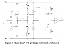
Taht is a "H-bridge", also called "quad-core" or a double diamond if you like.
A "current on demand" voltage feedback inputstage.
A "current on demand" voltage feedback inputstage.
Taht is a "H-bridge", also called "quad-core" or a double diamond if you like.
A "current on demand" voltage feedback inputstage.
Thanks. Funny that I know the circuits but have to catch up on my nomenclature, in which there are three names for the same thing!
Question to Guru Wurcer. In his paper linked to earlier, Ramus says this:
"Comparing Voltage and Current Feedback Op Amps: Two parts on the same process, at the same quiescent power, will have pretty similar open loop gain curves for VFB and CFB devices – Compare the OPA690 (VFB) and the OPA691 (CFB) below"
Why would he say that? Does a given process and power budget ultimately limit the attainable bandwidth/gain from a device?
Jan
I'm not sure this is the point to take away from the above. Raw speed/power is usually related to the process in some way and the benchmark usually ends up being related to signal fidelity.
As was pointed out the statement above relates to a very specific case. A very large customer asked me to convert one of our CFA DSL drivers to VFA and with the same internal degeneration as Rf and tweak of the compensation the performance was essentially equal and set by the power/speed budget. The extra buffer is usually a trivial amount of the total power budget. I'll remind folks again that the heavy degeneration in the VFA usually brings degradation of DC specs like Vos, Aol, etc. just like with the CFA (of course not the -in current noise).
If you look at a classic LTP VFA vs CFA on the same process compare the AD811 to the AD797. If DC precision is what you want you can use tricks and matching but usually you would only bother in a VFA (different applications). Some will remember the long gone AD846 which was an attempt at a "precision" CFA which failed in the market.
- Home
- Amplifiers
- Solid State
- Current Feedback Amplifiers, not only a semantic problem?