OK, I found the Alfet parts which might probably be similar to Exicon's.
They are SEMELAB ALF16N16W and SEMELAB ALF16P16W.
They are more expensive than Exicon parts, but at least there is another part that can be used, apparently.
They are SEMELAB ALF16N16W and SEMELAB ALF16P16W.
They are more expensive than Exicon parts, but at least there is another part that can be used, apparently.
I don't know why the rated specs are different, but it is the same die, and the datasheets use the same curves.
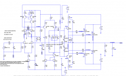
The schematic is now decided... did some modifications in the psu for the front end and increased rail voltages.
Now working in the pcb layout... will post results soon.
Now working in the pcb layout... will post results soon.
Finally some work done in the layout.... would apreciate your comments.
The layout corresponds to the latest sch where I modified the ltp ccs and mirror.
The vas mirror was also modified.
Some caps where added and now the IPS works at 75Vdc while the output at 63Vdc.
The layout corresponds to the latest sch where I modified the ltp ccs and mirror.
The vas mirror was also modified.
Some caps where added and now the IPS works at 75Vdc while the output at 63Vdc.
Attachments

Well, besides the obvious supply traces, I am not sure the usual custom of doing a ground plane is necessary or even useful.
Larger traces mean less resistance, so after I finish a pcb design I go over the whole design again widening the traces I did, and sometimes filling the empty areas with copper from whatever is closer. So I end up with a large copper surface cut by 1 to 2mm "streets" or "rivers".
That allows different position or size for passive components, or even using SMDs or through-hole if you prefer.
When I started doing this I asked around to professional pcb designers, and there was nothing against that, on the contrary.
But maybe someone here has a different opinion here that I would love to listen to.
Cool... will be widening traces wherever possible.. It is good to have low resistance traces.. As for ground planes... in a power amp maybe it is not needed
Many people have told me that ground planes were not necessary in audio, except maybe in very low noise circuits or certainly in DACs and similar.
Just curious. Have you (or anyone) had a look at those dual FETs made by InterFET and sold by Mouser? Might be a good choice for the LTP pair.
The IFN411 looks quite interesting and reasonably priced ($6.75 ea.).
They don't specify match % between the two FETs though.
The IFN411 looks quite interesting and reasonably priced ($6.75 ea.).
They don't specify match % between the two FETs though.
Just curious. Have you (or anyone) had a look at those dual FETs made by InterFET and sold by Mouser? Might be a good choice for the LTP pair.
The IFN411 looks quite interesting and reasonably priced ($6.75 ea.).
They don't specify match % between the two FETs though.
Thank you for the tip..... will look into it
A 360° turn and now the final version is here.....
Why did you change the VAS stage?
- Status
- Not open for further replies.
- Home
- Amplifiers
- Solid State
- Very HQ power amplifier (Assemblage VII)