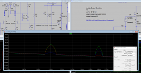
Can you explain something? What does C3,C4,R19 network? And why middle point of the biasing chain is connected to out net?
I increased current in LTP and reduced it's loading resistors.
Changed the mirror transistors and reduced output iddle current.
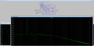
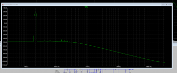
Now I have an almost good FFT at 20khz.
Gain is near 32dB.... good for a unity gain preamp 🙂
I tried to lower Vdrain at the 2sk170 to 11v using a 12v zener but could not make it work.
I would like to use faster devices for Q5 and Q6 but do not know what to choose..... can you help ?
I will build this rig soon....
Changed the mirror transistors and reduced output iddle current.
Now I have an almost good FFT at 20khz.
Gain is near 32dB.... good for a unity gain preamp 🙂
I tried to lower Vdrain at the 2sk170 to 11v using a 12v zener but could not make it work.
I would like to use faster devices for Q5 and Q6 but do not know what to choose..... can you help ?
I will build this rig soon....
Attachments
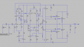
Now the working model...... It sports some Cordell ideas and just needs some imput related with V2 (6.3vdc).... how can I replicate this voltage source in real components in the circuit ?
Attachments
No degeneration on the outputs, so better have matched devices for each rail in the real build...
Ok.... I believe I have a good basis.... now I will study the bootstrap on the drivers that I think is genial. The problem is that I do not have enough knowledge to determine the optimum operation points and I have a poor vision regarding what current components I should use in each placement.
Untill now I have been strugling to lower FFT gremlins at 20k but I do not understand why they appear in worst forms at 1K FFT.
Will also experiment with square and ramp waves in sensible points in the circuit but I am not sure I can have a good result without help from you guys.
For example... why should I use Rs values when paralelling lateral mosfets ? (I will match the devices) but I believe any Rs will cause distortion.
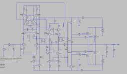
@ mcd99 .... please have a last look at my latest sch.
I kept the jfet cascode vref related to output as I do believe it is a very good procedure.
I believe I could have better results using speedy trannies as drivers so I wil experiment with the boostrap idea (I do hope the caps do not leave a significant signature) but maybe we could cascode the drivers..... would you help me here please ?
Also not sure about the optimum feedback values and input will be welcome.
I read that I could minimize output offset by loading the IPS LTP with a mirror but not sure the optimum currents I should use.....
And than there is the wondefull design Miib made for me "The Circle" that simulates much better and sports less than half the components.......
Need much input to decide....
Untill now I have been strugling to lower FFT gremlins at 20k but I do not understand why they appear in worst forms at 1K FFT.
Will also experiment with square and ramp waves in sensible points in the circuit but I am not sure I can have a good result without help from you guys.
For example... why should I use Rs values when paralelling lateral mosfets ? (I will match the devices) but I believe any Rs will cause distortion.
@ mcd99 .... please have a last look at my latest sch.
I kept the jfet cascode vref related to output as I do believe it is a very good procedure.
I believe I could have better results using speedy trannies as drivers so I wil experiment with the boostrap idea (I do hope the caps do not leave a significant signature) but maybe we could cascode the drivers..... would you help me here please ?
Also not sure about the optimum feedback values and input will be welcome.
I read that I could minimize output offset by loading the IPS LTP with a mirror but not sure the optimum currents I should use.....
And than there is the wondefull design Miib made for me "The Circle" that simulates much better and sports less than half the components.......
Need much input to decide....
Hi,
Personally, I always use bootstrapped drivers. It gives the VAS an easier time. Therefore, reducing distortion. Wouldn't worry about the electrolytics. They are driving the collectors of the drivers. The transistors themselves with give an element of rejection to any possible effects from the bootstrap caps. Anyhow, you have a nice big electrolytic in the feedback network. This would be a much bigger factor?
You could cascode the drivers but don't really see any gain here. Bootstraps will be fine.
Have looked at your latest .asc and have changed the transistors to the ones that I would use. Also, don't like the mirror arrangement loading your VAS. There's not much to be gained from the second mirror. Remember reading somewhere on this site about possible oscillation from this arrangement.
Another thing to look into is DC servos. Then you could eliminate the feedback cap and use a low impedance feedback network. I use a 1k feedback resistor. If you change the feedback resistor, you will need to adjust your compensation components.
One last thing, G-D caps on the MOSFETs would allow the use of much smaller gate resistors. This would allow faster compensation and better THD at 20Khz with the same stability margins. Could get faster slew rates too.
Paul
Attachments
why did you put R36 and R37 in place ?
Also why did you reference the IPS CCS to the +Vcc ?
R36 and R37 limit the loop gain at lower frequencies. They also lower the output impedance of the VAS. You could set them up as shunts but feeding back to the input node is more efficient. No loop gain wasted.
Referenced the CCS to the other rail as it saves a 0V connection on a PCB.
Also, noticed another issue with your amp ( or at least my mcd version 😉). Reduce the degeneration of the VAS current mirror to 100R (R20 and R14). There isn't enough voltage across those transistors for the mirror to operate. Then check your FFTs....
Paul
Last edited:
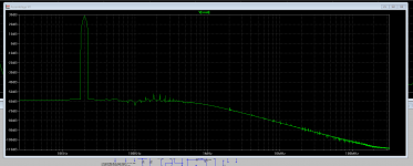
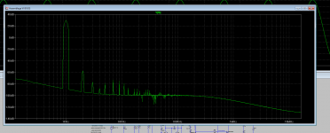
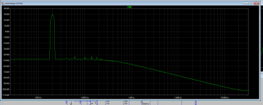
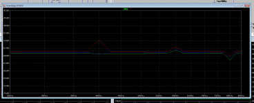
Been playing with R36 R37 and found that the optimum value would be 1.4meg if we want to null 2nd. at 1Khz
680k and no resistor at all produce the same 2nd but 3rd decreases without the resistors.
Pics show FFT with:
Green - 700k
Blue - 1.4Meg
Red 2000meg
680k and no resistor at all produce the same 2nd but 3rd decreases without the resistors.
Pics show FFT with:
Green - 700k
Blue - 1.4Meg
Red 2000meg
Attachments
Last edited:
- Status
- Not open for further replies.
- Home
- Amplifiers
- Solid State
- Very HQ power amplifier (Assemblage VII)