B-C always intact...
Use to come across this type of fault on many occasions, be it discrete low voltage regs or video output transistors etc.... and it always seemed to be the 2SA's and 2SC/D's etc.
Sometimes intermitant OC too.
Never any contributing factors... they just went OC and we always fitted BC/BD/TIP replacements etc... with no further trouble.
Hi CBS240 and Piercarlo,
very interesting to read, the comments about post #296, #297 and #298.
Perhaps this could be the reason, that there are really no books, application notes and literature about various emitter structures in Audio power bipolare junction transistors - the actual purpose to start this thread already in the summertime (July 2009).
But I discover an interest article, title:
"The 2N3055: a case history" mentioned about
IEEE Xplore - Login
Perhaps this article was posted here about diyaudio. But I get no suggestions about google to this forum. Thank you for an advice.
Last edited:
I'm almost certain that the 0.01% amp was with those old MJ's but I'd have to look it up (all I have on hand ATM is the THD plot). Can't remember if it was a CFP OPS or not. However it's after 4am ATM, so I'm going to bed now instead.
Regarding the MOSFET comparison, my claim is for a pair. If I recall correctly your EC amp did in the vicinity of 0.02% - 0.030% THD20 without the EC? That was with a 2MHz ULGF, right? The EC was more effective than 24.4dB? (0.01%/0.0006%)
What was that biased at?
Cheers,
Glen
Hi Glen,
You're about right about the MOSFET amp. I was built with first generation HEXFETs biased at 150 mA, with no source resistors. It had about 2 MHz gain crossover, and the EC at 20 kHz improved matters by almost 30 dB. THD 20 with EC was 0.0006%, so that would imply THD without EC on the order of 0.02%.
I have also regularly built MOSFET amps (IRFP240/9240) without EC and similar bias with 1 MHz BW with THD-20 less than 0.03%. Amps based on the Toshiba MOSFETs will come in a little lower in THD. A little bit of source resistance carefully chosen (and not necessarily the same for P and N) can reduce THD a bit further.
Cheers,
Bob
Self is a very good professional in audio amplifiers design. BUT, he only concentrates on non-linear distortions (THD, IMD). He does not care much about speed and ultimate stability, he does not care about symmetry of rising and falling edges, he does not care about hard clipping. His design has +, but - as well. Nothing is perfect.
PMA,
Well-stated. As you know, I do believe in achieving low THD as well. If THD-20 is very low, it does not leave a lot of wiggle room for other HF nonlinear distortions. However, I also believe strongly that it matters how you get there. You want to get to that low value of THD-20 with an open-loop design that is very linear, well behaved and stable in the first place. The amplifier also should have very civilized behavior in the closed loop, such as symmetry and lack of sticking and overhand in clipping. It is also very important that the amplifier retain these good qualities in low-impedance loads and loads with reactive load lines.
Low THD is good, but one should not sacrifice or ignore other behavior to achieve it.
Lastly, there are different kinds of low THD-20. If it is only measured in an 80 kHz bandwidth, it is far less meaningful and impressive. It should be measured in a 200 kHz bandwidth, and ideally its spectral components should be evaluated. This is problematic absent a spectrum analyzer that can see out to 200 kHz (10th harmonic). This is why I usually prefer 19+20 kHz CCIF with full spectral analysis. Sadly, I don't think Doug has shown such measurements.
Cheers,
Bob
As you know, I do believe in achieving low THD as well. If THD-20 is very low, it does not leave a lot of wiggle room for other HF nonlinear distortions. However, I also believe strongly that it matters how you get there. You want to get to that low value of THD-20 with an open-loop design that is very linear, well behaved and stable in the first place. The amplifier also should have very civilized behavior in the closed loop, such as symmetry and lack of sticking and overhand in clipping. It is also very important that the amplifier retain these good qualities in low-impedance loads and loads with reactive load lines.
Bob,
completely agreed.
Regards,
B-C always intact...
Use to come across this type of fault on many occasions, be it discrete low voltage regs or video output transistors etc.... and it always seemed to be the 2SA's and 2SC/D's etc.
Sometimes intermitant OC too.
Never any contributing factors... they just went OC and we always fitted BC/BD/TIP replacements etc... with no further trouble.
A second breakdown triggered avalanche seem to be the most probable cause. A way for understanding how second breakdown cause the fault is thinking of it as a machinery that lower maximum junction temperature allowance with the increase of Collector-Emitter voltage. A relatively "rugged" device at low working Vce, cease quite rapidly to be "rugged" when Vce go up to higher levels. A good image of problem is thinking power devices as "silicon" devices at low working voltage which rather quickly turn into "germanium" devices with Vce increasing.
Example: a 2N3055 is a "silicon" device until 40 Volt of Vce and turn into a "germanium" device as it approaches its upper voltage limit, with an effective junction temperature that should not steadily pass 80-90 °C otherwise second breakdown overheating start to build-up.
(BE CAUTIOUS: Don't take this as a "truth" but just not more than of a useful trick thinking when coping with effective power limits of bipolars).
Hi
Piercarlo
Perhaps this could be the reason, that there are really no books, application notes and literature about various emitter structures in Audio power bipolare junction transistors - the actual purpose to start this thread already in the summertime (July 2009).
But I discover an interest article, title:
"The 2N3055: a case history" mentioned about
IEEE Xplore - Login
Perhaps this article was posted here about diyaudio. But I get no suggestions about google to this forum. Thank you for an advice.
I've tried to get that document from other sources but i found nothing, sorry!. However i think that the kind of information you search are retrievable only applying directly some form of reverse engineering on die layouts, with the assist of a bold knowledge about process and technology employed in transistor manufacturing (and this may be helped by some books as that written by Roulston, "Bipolar Semiconductor devices").
Also data specified in datasheet may provide an indirect insight about inner structure of devices and some empirical measurement ot typical c-b or b-c capacitances as those you signalled in other thread, provides some clues about that - mainly about the way routed for achieving some purposes... but that's all.
I don't trust much in the public availability of the most of the informations you are looking for. Informations that are, for the most, surely patented. Pheraps on Patent Office databases may be retrieved something... but its a really daunting task getting riddle of their huge contents! :-(
Hi
Piercarlo
A second breakdown triggered avalanche seem to be the most probable cause. A way for understanding how second breakdown cause the fault is thinking of it as a machinery that lower maximum junction temperature allowance with the increase of Collector-Emitter voltage. A relatively "rugged" device at low working Vce, cease quite rapidly to be "rugged" when Vce go up to higher levels. A good image of problem is thinking power devices as "silicon" devices at low working voltage which rather quickly turn into "germanium" devices with Vce increasing.
Example: a 2N3055 is a "silicon" device until 40 Volt of Vce and turn into a "germanium" device as it approaches its upper voltage limit, with an effective junction temperature that should not steadily pass 80-90 °C otherwise second breakdown overheating start to build-up.
(BE CAUTIOUS: Don't take this as a "truth" but just not more than of a useful trick thinking when coping with effective power limits of bipolars).
Hi
Piercarlo
One explanation for secondary breakdown is that as Vce increases, the depletion region between the base and collector becomes wider, intruding on the base and making the base thinner. This causes a greater likelihood of differences in current across the die (note that beta gets higher as base gets thinner, and current becomes more sensitive to base thickness). When there becomes a non-uniform distribution of current across the die, those areas that are conducting more current get locally hotter.
The Vbe of those hot spots goes down due to TCvbe, causing them to conduct still more current, quickly leading to a localized thermal runaway condition that results in device destruction.
Bob
hi bob:
a potentially interesting approach. might you be willing to say more about this? sounds like you've played around with it a bit ...
mlloyd1
a potentially interesting approach. might you be willing to say more about this? sounds like you've played around with it a bit ...
mlloyd1
Hi Glen,
... A little bit of source resistance carefully chosen (and not necessarily the same for P and N) can reduce THD a bit further.
Bob
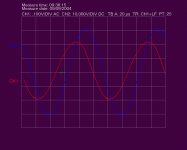
These are oscilloscope captures from a typical class AB circuit with composite VAS, optimum bias, class A drivers, switching speed-up capacitor across the bases of output devices, low inductance emitter resistors, low inductance layout, etc...
The VAS is driving BD139/BD140, then TIP35C/TIP36C at 4 ohm and 10khz.
CH1 is VAS current, mostly dominated by VAS compensation capacitor current, but revealing the non linearities due to switching. Nowadays I would have taken the effort to remove capacitor current in order to show output stage non linearity more clearly. Increasing or decreasing bias resulted in worse waveforms.
CH2 is output voltage.
The 4Mhz Ft of output devices is noticeable But with a bad layout with high inductances and inductive output resistors it could be much worse...
Note that this is 5 year old work.
Attachments
Last edited:
Good morning,
there´s not much I like about Douglas Self`s views, the theory of optimally biased class B is not an exception. Besides switching distortion, crossover distortion consists of a large number of components, most of them device-specific. Resistances in the base-emitter path stabilize some variables, a lower Vbe excursion improves the generally poor Vbe/Ice relationship, but increase the switching time, thereby crossover distortion. Output stages should be class A biased for normal listening power levels.
The blameless amplifiers necessarily have poor subjective quality and high distortion, even if it´s beyond measurement boundaries, no matter how many chapters are written in support of the opposite. The open-loop properties set the pertinent values, the rest is a bubble. Disconnect the closed-loop and make your measurements, an amplifier is never better than its open-loop.
Resistance in the base-emitter path makes switching worse, or at least slower.
Switching behaviour of bipolar transistors is not that hard to understand (at least when you have used them for plain switching and fine tuned these circuits). Base-emitter capacitances when some collector current is being conducted becomes quite high due to charge storage. Real world current gain is strongly time dependent and is low in the low current region for some devices.
When output current is increasing from negative to positive in order to shift from PNP to NPN and the less than 1A or so IC is reached, current gain starts to roll off so base current does not fall linearly with output current, then current crosses zero and a positive current pulse is required to remove the remaining charge stored in PNP b-e junction and store some charge in NPN b-e junction. Then, current gain starts as unity and gradually increases to DC gain within a few microseconds depending on Ft of output devices. And vice-versa.
Fast local error correction at the input of the output stage can prevent the voltage amplifier stage from seeing most of that non-linear stuff. However, in the usual amplifier topologies (in which most people has been stuck for ages), the dominant pole compensation of the VAS does the opposite of what would be required for optimum switching, it tries to "reconstruct" the expected output waveform at the input of the output stage, where spikes *must* exist due to the nature of class AB, rather than at amplifier output.
The inductance of output resistors, transistor packages and PCB traces also plays a role, a voltage equal to L*di/dt appears across these inductances. The base current spikes result also in voltage spikes due to these inductances. But this is not necessarily a terrible thing, for example, in class D amplifiers I use this parasitic inductance (mostly from TO-220 packages due to the chip capacitors directly from TO-220 leads to power planes) to get a regulated di/dt, the rate at which current rises and falls, regardless of supply voltage and temperature.
I wish most people writing here had some background on high speed switching electronics. Simulating linear circuits does not tell about many details.
Last edited:
Eva,
If anything. Not showing real-world events in function of time makes static analysis nearly worthless.Simulating linear circuits does not tell about many details.
Resistance in the base-emitter path makes switching worse, or at least slower.
Yes it does, Rb base stoppers make switching slower.
hi bob:
a potentially interesting approach. might you be willing to say more about this? sounds like you've played around with it a bit ...
mlloyd1
Hi Mlloyd1,
The use of source resistors in a MOSFET output stage can sometimes help achieve a better compromize in the crossover distortion region, where transconductance droop occurs. First, the source resistors reduce somewhat the much higher transconductance exhibited by the MOSFETs at high currents outside the crossover region. Secondly, the P and N-channel MOSFETs often have somewhat different amounts of transconductance for a given amount of bias current. This can cause asymmetry in the crossover region. If slightly different values of RS are used for the P and N devices, a better balancing compromise can sometimes be achieved. We are not talking about large values of source resistance here - always less than 1 ohm. We certainly do not want to give up too much voltage swing headroom under high-current conditions.
I have to emphasize that this approach depends a lot on the individual characteristics of the P and N MOSFETs used, and does not necessarily yield really big improvements. I usually employ source resistors anyway for current monitoring and protection, so it only makes sense to tweak them for best performance if they are there anyway.
Less improvement will tend to result when better P/N matched MOSFETs are employed, like the Toshiba devices.
BTW, the addition of reasonable-sized source resistors does not usually do a lot to improve quiescent bias current matching among paralleled devices.
Cheers,
Bob
Yes it does, Rb base stoppers make switching slower.
Agreed. Base stoppers can also impair bias stability and alter the optimum class AB bias current for a given size of emitter resistance. They also add a pole to the transconductance characteristic. It should not be overlooked that the base stoppers effectively add to the intrinsic base resistance of the power transistor, which is usually on the order of a couple ohms for small signals. However, emitter crowding causes intrinsic base resistance to decrease at higher current. This change can alter the output stage stability conditions as current changes.
It is a delicate tradeoff, but it is best to keep base stopper resistance as small as possible while retaining adequate stability over all conditions.
Cheers,
Bob
The blameless amplifiers necessarily have poor subjective quality and high distortion, even if it´s beyond measurement boundaries, no matter how many chapters are written in support of the opposite.
Cool...almost a religious statement...
regards,
The blameless amplifiers necessarily have poor subjective quality and high distortion, even if it´s beyond measurement boundaries, no matter how many chapters are written in support of the opposite.
I use often the blameless amplifier topology (to modify existing amplifiers) for driving low frequency transducers, because I get a very tight and clean bass reproduction. Regarded the upper frequency range the poor subjective quality I also always observe, because I hear harshness by reproduction of voices e. g. Pure class-A concepts with only local NFB are clearly better there (e. g. the ZEN or Aleph topology). To use the blameless amplifier topology for full range applications isn't a royal way, except I prefer only rock music or very hard techno beats and no acoustical jazz or classic.
What means "almost a religious statement" ??
This term I have never heard before in this case
Cool...almost a religious statement... regards,
I use often the blameless amplifier topology (to modify existing amplifiers) for driving low frequency transducers, because I get a very tight and clean bass reproduction. Regarded the upper frequency range the poor subjective quality I also always observe, because I hear harshness by reproduction of voices e. g. Pure class-A concepts with only local NFB are clearly better there (e. g. the ZEN or Aleph topology). To use the blameless amplifier topology for full range applications isn't a royal way, except I prefer only rock music or very hard techno beats and no acoustical jazz or classic.
What means "almost a religious statement" ??
This term I have never heard before in this case
Last edited:
The blameless amplifiers necessarily have poor subjective quality and high distortion, even if it´s beyond measurement boundaries, no matter how many chapters are written in support of the opposite. The open-loop properties set the pertinent values, the rest is a bubble. Disconnect the closed-loop and make your measurements, an amplifier is never better than its open-loop.
The distortion is 0,01%-20KHz to 30dB NFB (~32x in unity gain). this results in a distortion less than 1% in open-loop, that is good for simplicity. I would like to know your method to measure the distortion in open-loop.
BTW: there is a way optimally biased for drivers?
- Home
- Amplifiers
- Solid State
- bipolar (BJT) transistor families for audio power output stages