Hi Glen,
I don't recall Self achieving 0.01% THD-20 with MJ802 devices (which I also don't think were 4 MHz ft). I'll have to go review what he did and what he achieved.
Is suspect if he did it, it was with his beloved CFP output stage, which is very picky with quiescent bias, and in which he actually starves the output transistors to achieve proper crossover.
In any case, I agree that a good design with 21193/4 devices can achieve 0.01% THD-20.
A generously-biased MOSFET amp can also achieve that number without EC, but it will have somewhat higher idle dissipation. Two pair of vertical MOSFETs, each pair biased at 150-200 mA, combined with a 1 MHz gain crossover frequency, will do it. Such a design will not suffer nearly as much trouble with thermal stability and distortions due to junction temperature variations inflicted by program material.
Cheers,
Bob
I'm almost certain that the 0.01% amp was with those old MJ's but I'd have to look it up (all I have on hand ATM is the THD plot). Can't remember if it was a CFP OPS or not. However it's after 4am ATM, so I'm going to bed now instead.
Regarding the MOSFET comparison, my claim is for a pair. If I recall correctly your EC amp did in the vicinity of 0.02% - 0.030% THD20 without the EC? That was with a 2MHz ULGF, right? The EC was more effective than 24.4dB? (0.01%/0.0006%)
What was that biased at?
Cheers,
Glen
I think Dougs figures were well below 0.01% and nearer 0.003% ? at 20khz with the MJ's
yes, with a MJ802/3502 pair...
0.004% at 20 KHZ and 0.001% in midrange...
truly very low values...
Take tons of feedback and you are there. How worthful? Not sure that the THD race has any sense.
Take tons of feedback and you are there. How worthful? Not sure that the THD race has any sense.
Many things in audio are devoid of any sense. But the show must go on... ;-)
Hi
Piercarlo
Try it, and post Your results 😛. It has the same sense, as race for SR about 300V/us. Maybee than it is better to use Schmit trigger🙂.Take tons of feedback and you are there. How worthful? Not sure that the THD race has any sense.
Take tons of feedback and you are there. How worthful? Not sure that the THD race has any sense.
BTW, "tons of feedback" in graph I posted means about 25dB LG in whole band from DC to about 40kHz. Low THD(20) means low IMD also, and this has much more sense,as plain THD.
Last edited:
Doug made an interesting comment years ago 🙂
That if you want a "different" sound, then you should introduce that as a device to distort the signal in some way (add even harmonic distortion etc) before the "blameless amp". I think he called it a niceness control lol
Sadly my experience has taught me it's not quite that simple... and no "niceness" circuit was ever forthcoming.
An interesting idea though... don't ya think !
Self is a very good professional in audio amplifiers design. BUT, he only concentrates on non-linear distortions (THD, IMD). He does not care much about speed and ultimate stability, he does not care about symmetry of rising and falling edges, he does not care about hard clipping. His design has +, but - as well. Nothing is perfect.
Self is a very good professional in audio amplifiers design. BUT, he only concentrates on non-linear distortions (THD, IMD). He does not care much about speed and ultimate stability, he does not care about symmetry of rising and falling edges, he does not care about hard clipping.
Very well said.
The biggest problem IMO in his designs is the use of global feedback.
Take it out and those THD figures stop looking so awesome 😉
Self is a very good professional in audio amplifiers design. BUT, he only concentrates on non-linear distortions (THD, IMD). He does not care much about speed and ultimate stability, he does not care about symmetry of rising and falling edges, he does not care about hard clipping. His design has +, but - as well. Nothing is perfect.
That's not entirely true. In part of his book he is trying to investigate the reasons of unequal slewing and how to deal with it. As of speed and stability we all have different expectations and standards. But, nevertheless, there is plenty of information and guidelines in his books. I almost sure that majority of us have read his books (or articles), but I am amazed how much design flaws are floating around in some amplifiers in this forum and they pass by unnoticed.
Cheers
Has anyone seen the base current waveforms of the output devices in a class AB output stage while sourcing/sinking high current at anything but bass frequencies? They usually look horribly distorted, with turn on and turn off spikes and 25%-50% non-linearity. And I don't mean in simulation, I mean probing in prototypes.
This is the reason, why nobody a certainly level of sonic transmission quality can never exceed by the use of class AB with typical value of idle current between 30 and 50mA through the output power devices, even with the best available voltage driver topology of the world and independend the question, whether the use of global NFB now is better or not.
If you all read the follow article carefully, you will understand, why pure class A and class AB will give much more different in sonic quality than the question, how value of Ft for the output devices is neccesary at least:
http://www.firstwatt.com/downloads/seclassa.pdf
The sonic different between old Texas TIP2955/TIP3055 and Sankens 2SC2922/2SA1216 (a little less harshness) is clearly audible but not dramaticly at class AB and negligible in pure class A mode (I have testet this by the circuit topology from the circuit about post #1 about
http://www.diyaudio.com/forums/solid-state/122378-cambridge-audio-a3i-repairs-mods.html ).
But the sonic different between Class AB and Class A is dramaticly in the upper frequency range above approximately 500 - 1000 Hz
The challenge must be to find a high speed voltage driver, that can cancel all odd and high order THD components causes through crossover distortion effects by low idle current values through the output power devices (so I can speak from a virtual Class A).
But I doubt very much whether this is possible independend of the kind of circuit topology, the value of Ft or the feedback question.
Since after more than 50 years solid state amplifier engineering still can't nobody demonstrate such amplifier with a small quiescent current, which can not be distinguished to pure Class-A versions, must be my doubts right.
Thus EVA's statement is right regarded Class D.
For me still the royal way is the distribution of different modes in different frequency ranges - pure Class A in the upper and AB in the lower range, because harsh sonic transmission isn't important, because inaudible by the heavy cone resp. diaphragm for the low frequency transducer. Here the damping factor and dynamic behavior of power supply must be appropriate values.
To use one amplifier for the whole frequency range is always a compromise regarding the max. possible transmission sonic/sound quality, even by use of the best available devices and topologies and even by pure class-A mode. This will unfortunately always overlooked.
Last edited:
To use one amplifier for the whole frequency range is always a compromise regarding the max. possible transmission sonic/sound quality, even by use of the best available devices and topologies and even by pure class-A mode. This will unfortunately always overlooked.
Absolutely agreed. For low midrange (100-400hz) i think that plain class B (not AB) can be preferred.
weinstro,
after having read some articles about Japanese transistors, I made my first investigation back in the eighties. At that time I was constantly modifying things, executing listening test on passive and active components, various topologies, using easily interchangeable plug-in modules. (Unfortunately, I`m much more lazy now). It was not hard at all to notice the difference, in short, considerably less hash in the upper frequency range.
Again, precision in manufacturing is crucial, especially when complex processes are used. I only trust original manufacturing. Why manufacture other`s superannuated stuff`? Certainly not to make it better. I would manufacture my own stuff that is better, no?
Hi Eva,
Switching gives rise to the worst distortion in amplifiers. The switching action creates highly annoying transients and brings about rapid changes in control voltage, triggering high slew rates and peak currents not just in the driver stage but in all stages in the loop. Missing gain in the cut-off and high frequency region and various transition anomalies do not mitigate the situation. There`s no way to iron out all that.
Switching and linear audio is a bad combination.
Regarding a previous issue:
The switching performance determined by the time required to establish voltage changes across capacitances.
Note: same capacitance values do not mean same switching performance in different devices.
I agree with your description, but not your conclusion.But class AB does require fast output transistors because it's by definition a mix of switching and linear amplifiers. The output stage is switching every time speaker current crosses zero amperes in either direction. Class G and class H have exactly the same requirement, but with additional switching points.
Traditionally these amplifiers require lots of feedback for linearisation, either global or disguised as local to keep some people pleased.
Has anyone seen the base current waveforms of the output devices in a class AB output stage while sourcing/sinking high current at anything but bass frequencies? They usually look horribly distorted, with turn on and turn off spikes and 25%-50% non-linearity. And I don't mean in simulation, I mean probing in prototypes.
But, if mixing linear with switching is the problem, why not just going full switching? Nowadays we have excellent switching devices. Open loop linearity is far better, like in class A, and not much negative feedback is applied (or can be applied, that's one of the problems, or advantages, or challenges... )
Switching gives rise to the worst distortion in amplifiers. The switching action creates highly annoying transients and brings about rapid changes in control voltage, triggering high slew rates and peak currents not just in the driver stage but in all stages in the loop. Missing gain in the cut-off and high frequency region and various transition anomalies do not mitigate the situation. There`s no way to iron out all that.
Switching and linear audio is a bad combination.
Regarding a previous issue:
The switching performance determined by the time required to establish voltage changes across capacitances.
Note: same capacitance values do not mean same switching performance in different devices.
Has anyone seen the base current waveforms of the output devices in a class AB output stage while sourcing/sinking high current at anything but bass frequencies? They usually look horribly distorted, with turn on and turn off spikes and 25%-50% non-linearity. And I don't mean in simulation, I mean probing in prototypes.
Hi
This is a good point. The distorted drive waveforms really throw a kink in the transfer function wrt the "wire with gain" goal, and conventional feedback is not going to eliminate all of this distortion at the output.
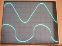
For example, you can see the gate drive with all of the distortion, or rather the error that is corrected for in these waveforms from my EC fet amp...(the sine wave is the output
 )100KHz and 200KHz
The errors are exaggerated in the fast signal, but at audio frequencies, they are still there.
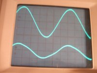
As for crossover, the drive distortions are specific. The attached photo shows the output waveform (30KHz) of a heavy class B bias OPS and the difference from the output signal or rather the 'error' signal, required at the gates to produce it. Notice the slope of the EC drive signal around the crossover notch, and the distortion is still visible at the output. This is the 'error' Eva is referring too pertaining to crossover switching. The relatively limited BW of the global closed loop prevents correction of much of the switching distortion, which is where high BW local feedback/feedforward comes into play.🙂 The second photo is with 300mA of bias, yet the distortion is still there as indicated by the change in slope of the error signal around crossover. As you can see even with significant bias, crossover switching distortion is still an issue.


Attachments
Again, precision in manufacturing is crucial, especially when complex processes are used. I only trust original manufacturing. Why manufacture other`s superannuated stuff`? Certainly not to make it better. I would manufacture my own stuff that is better, no?
First: are you sure that actual "japanese transistors" are really japanese again? I should be not so sure... As certainly i'm not sure of "occidentality" of Motorola-Onsemi discrete devices (mexican plants are going to be closed if they are not YET close). And not to mention Fairchild which most of bipolars (even signal!) are just japanese equivalents of occidental devices, not "true" ones.
Second: precision in manufacturing semiconductors is MANDATORY for anyone want build anything as simple as may be a common planar diode. And this is similar for all semiconductors producers (i.e. again limited by physical issue). That really differ is not precision in manufacturing but just SELECTION in post manufacturing. In this field japanese excel (and not only in semiconductor buildings) but, at least in semiconductors industry, other dont stay at window to see the landscape. This because nowadays silicon foundries for basic products as discrete transistors and general purpose linear are exactly the same, or at least located in the same place, for japanese as for rest of world manufacturers.
In other words, your claim for japanese excellence has become a myth from long time ago... and still going onward to became more mythical again.
Japan has suffered, last year, the worst economic crisis after USA... And this don't made you rise any suspect about the fact that "japanese golden age" has been (long) gone? No?...
Mah...
Piercarlo
I agree with your description, but not your conclusion.
Switching gives rise to the worst distortion in amplifiers. The switching action creates highly annoying transients and brings about rapid changes in control voltage, triggering high slew rates and peak currents not just in the driver stage but in all stages in the loop. Missing gain in the cut-off and high frequency region and various transition anomalies do not mitigate the situation. There`s no way to iron out all that.
Switching and linear audio is a bad combination.
Pheraps you'll be surprised to know that your "excellent superior japanese transistor" are just derived from an high voltage switching technology (triple diffused) developed by Siemens (NOT a japanese company...) for obtaining complementary high voltage switching devices (for application in three-phase servo-motor controllers). That technology was short lived in his original field of application because, in a few years turn, was outperfomed by other more apted devices (first MOS and after a bunch of years again, GTOs and IGBTs).
This lead a dismiss of triple diffusion as switching technology, but was promptly recovered as "audio" technology: Hfe were low but linear; Ft well promising, starting from a 20 MHz minimum; switching time were not of "speedy gonzalez" type (after all we are dealing again with bipolars, not MOS!) but were really better than of its predecessor.
When Toshiba entered the european market with some joint-ventures with Siemens and ST (mainly with the goal of turning around the "de facto" protectionist policy applied at time by ECC by "slugging" the direct entering of high tech products from Japan and other "too cheap" asian manufacturing countries), buy triple diffused technology at very favurable price, discard its original field of application for what owned the development of more promising technologies, and improve some of its details in view of producing and marketing "audio transistors", at start only for japanaese or japanese controlled markets, where existed a "true" industrial audio background able to grasp the essence of novelty and use it. Really not a good move for european side of business...
That's all...
Regarding a previous issue:
The switching performance determined by the time required to establish voltage changes across capacitances.
Note: same capacitance values do not mean same switching performance in different devices.
Especially if "capacitances" in semiconductors are not capacitances at all but near constant charges. Do you know "varactor effect"?
BTW: "modern japanese devices" are more "capacitive" than "old occidental devices". This should be a clue of fact what "capacitances" are not the whole story to tell...
Piercarlo
Just going slightly off topic... I noted that small and medium signal Japanese transistors in consumer gear of the 1980's and 90's often failed open circuit base emitter for some strange reason.
Just going slightly off topic... I noted that small and medium signal Japanese transistors in consumer gear of the 1980's and 90's often failed open circuit base emitter for some strange reason.
Base-collector junctions were still working? If so a surge current in collector-emitter circuits has occurred and melt-off the emitter physical commection. Causes of that may vary from an upset in supply voltage to an overheating what triggers a second breakdown issue (is not a nuisance of power bipolars only!). There is not a single exhaustive answer...
Hi
Piercarlo
- Home
- Amplifiers
- Solid State
- bipolar (BJT) transistor families for audio power output stages