Kozard, I note that your plot shows noise content is circa -30dB below H2 level, but the results box displays N as -110dBFS. Perhaps an issue for you is related to units and what units you have chosen. There could also be a bandwidth issue. Could be worth playing around with settings.
What setting would you suggest looking at? Nothing jumped out at me in the distortion settings menu or the preferences.
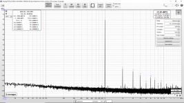
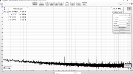
The results box says -110 dBFS and the graph shows noise at -140 to -150 dBFS. It seems odd since both are dBFS. It should line up since they are both the same units?
The results box says -110 dBFS and the graph shows noise at -140 to -150 dBFS. It seems odd since both are dBFS. It should line up since they are both the same units?
Perhaps change every setting you can see (eg. in the graph controls panel - top right icon - including all the subsettings like coherent averaging - and read the help on each, as a learning curve). Once you have a fair handle on what changes occur and why, then perhaps post over on the REW forum showing what you are getting and what values you don't understand why you are getting. The outcome could be a variety of reasons, such as an unknown setting is not appropriate, or you didn't appreciate a particular setting's consequence, or there is a bug, or ......
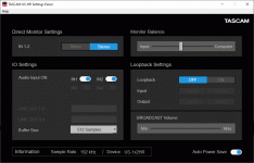
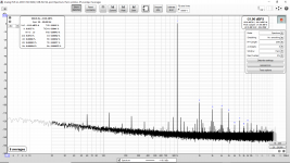
In my previous measurements of the Tascam US-1x2HR I used the internal loopback.
Here are the measurements with an external loopback (RCA out connected to RCA in).
Best results I got is with ASIO 192k, REW generator -10db, Tascam Line out volume at 2 o'clock.
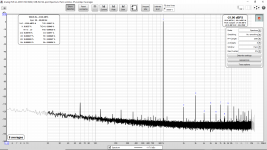
Here are the measurements with an external loopback (RCA out connected to RCA in).
Best results I got is with ASIO 192k, REW generator -10db, Tascam Line out volume at 2 o'clock.
Attachments

The N (noise and non-harmonic distortion) figure is the sum across the bandwidth, either as a ratio if the Y axis units are set to dBc or as a level in the current Y axis units.The results box says -110 dBFS and the graph shows noise at -140 to -150 dBFS. It seems odd since both are dBFS. It should line up since they are both the same units?
Yes, but in the attached RTA screen shot how can the sum add up to -110 dBFS?The N (noise and non-harmonic distortion) figure is the sum across the bandwidth, either as a ratio if the Y axis units are set to dBc or as a level in the current Y axis units.
Attachments
Last edited:
My input wiring is as follows:
- Input board with 2xRCA (ground joined for left and right)
I think that can be a problem. The grounds for the two L/R channels should only be common on the single star ground for the enclosure. Most builders use isolated (ground floating from the chassis) input jacks. The ground reference for the inputs will be on the amps' individual L/R PCBs. With multiple grounding points, you are creating a loop.
I am charging up the battery pack and I will try playing with the low pass and high pass in the distortion settings. Currently they are 20Hz and 20kHz.
I don't think there should be much (of interest) beyond that except for perhaps artifacts of the USB interface ADC/DAC? (E-MU 0404 USB?)
I will also take more RTA screen captures with the a wider frequency range. (Right now it is set to 20 to 20,000 using the button at the bottom right of the RTA display.)
Is there a reason to change the units? If not I will likely stick with dBFS. I could make a couple screen captures with dBc but I don't see why that would change the basic math question.
I think that can be a problem. The grounds for the two L/R channels should only be common on the single star ground for the enclosure. Most builders use isolated (ground floating from the chassis) input jacks. The ground reference for the inputs will be on the amps' individual L/R PCBs. With multiple grounding points, you are creating a loop.
I agree. I think that is the problem.
However with one power supply and two uPC1342V amplifier PCBs I don't see how to not create a loop. The uPC1342V PCB is designed with a star ground on the PCB for starters, then both of those (one for each amp) go to the rectifier/filter board. Then on top of that the two uPC1342V inputs are on separate boards with separate input ground reference terminals which first go to the individual amp PCB star ground layout and then the rectifier/filter board.
I don't think I can just attach the two input ground references to a chassis star ground because the PCB designer already connected various grounds (including the feedback network) to the star grounds on the two PCBs, which is a different point.
The problem goes away as a mono-block and I think it almost equally well solved by two independent power transformers and rectifier/filter boards.
There are a lot of FFT bins in that 20 kHz span, they soon add up.Yes, but in the attached RTA screen shot how can the sum add up to -110 dBFS?
I guess that is the answer. I guess it just integrates up to such a large number, especially with the LF (higher noise) integrated in.
It just seems very odd at first glance to look at noise at -150 dBFS and see -110 dBFS for noise.
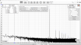
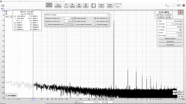
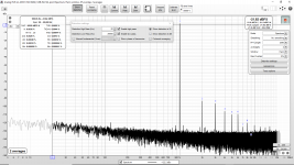
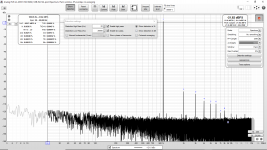
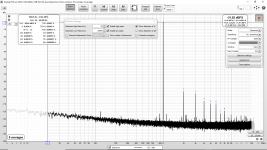
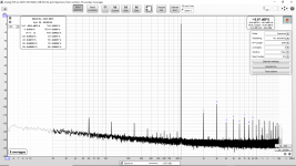
I did the following (attached) experiments with the distortion (HP high pass/LP low pass) and units (dBFS and dBc):
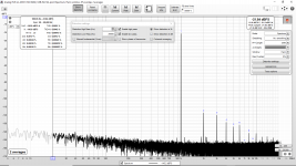
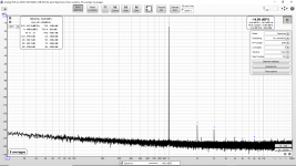
I also changed the display from 20 to 20k to 5 to 30k to show that there was nothing else of interest beyond the displayed bandwidth.
It just seems very odd at first glance to look at noise at -150 dBFS and see -110 dBFS for noise.
I did the following (attached) experiments with the distortion (HP high pass/LP low pass) and units (dBFS and dBc):
I also changed the display from 20 to 20k to 5 to 30k to show that there was nothing else of interest beyond the displayed bandwidth.
- Units dBFS, LP On - 20kHz, HP On - 20Hz, No Averages
- Units dBFS, LP On - 20kHz, HP On - 20Hz, 8 Averages
- Units dBc, LP On - 20kHz, HP On - 20Hz, 8 Averages
- Units dBc, LP On - 20kHz, HP On - 20Hz, No Averages
- Units dBc, LP On - 20kHz, HP On - 20Hz, 2 Averages
- Units dBFS, LP Off - 20kHz, HP On - 20Hz, 8 Averages
- Units dBFS, LP On - 20kHz, HP Off - 20Hz, 8 Averages
- Units dBFS, LP On - 20kHz, HP On - 20Hz, 8 Averages
Attachments
-
 Units dBFS 5 to 30k LP On HP On.png180.3 KB · Views: 147
 -
 Units dBFS 5 to 30k LP On HP Off.png167.9 KB · Views: 134
 -
 Units dBFS 5 to 30k LP Off HP On.png167.3 KB · Views: 128
 -
 Units dBc 5 to 30k LP On HP On.png178.4 KB · Views: 383
 -
 Units dBc 5 to 30k LP On HP On No Averages.png178.8 KB · Views: 392
 -
 Units dBc 5 to 30k LP On HP On 8 Averages.png159.6 KB · Views: 379
 -
 Units dBFS 5 to 30k LP On HP On 8 Averages.png159.6 KB · Views: 396
 -
 Units dBFS 5 to 30k LP On HP On No Averages.png165.5 KB · Views: 397
Last edited:
kozard, perhaps reducing the bandwidth would be a stronger confirmation that bandwidth was complicit in the higher than expected N value - part of the learning curve of what different settings may effect, or not.
I can try halving the bandwidth a couple of times and see how the summed/integrated N responds.
Any other specific suggested experiments that I should try?
Any other specific suggested experiments that I should try?
Perhaps read post #963 again. REW is a wonderfully powerful tool, but that can equally make it daunting to realise what particular settings influence as there can often be so many settings without an immediate way of knowing if any are important for an issue.
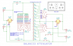
Stepped Differential Attenuator
I posted this over in the Equipment and Tools forum, but I thought it might be interesting to the folks in this thread.....
I got tired of cobbling together resistors to attenuate amplifier signals when doing distortion measurements. For low-level measurements, having a rats nest of parts and wires on the bench was bad from a noise standpoint as well.
So I decided to put together a fully differential stepped attenuator. I wanted:
1) Either fully differential or single-ended use (switchable)
2) XLR (mini) and BNC connectors
3) Coarse and fine adjustment
I looked around for an easy way (as opposed to something fancy like relays and R2R networks) to do this and came across Joe Broskie's clever idea of using a combination of shunt resistors for coarse adjust and a series string for fine steps. He sells a kit to do this on his Glass-Ware store. Currently, they appear to be out of stock.
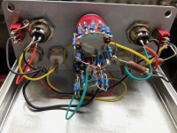
The first picture shows the completed unit in a small aluminum case. The second shows the schematic with resistor values and the third shows the internal (somewhat messy) point-to-point wiring. The resistors are mounted directly on the switches.
For the shunt resistors, I used 1%. For the input and series string resistors, I used 0.1% in order to keep common-mode errors low in balanced mode.
Note that the attenuator has an in-built 3 dB insertion loss due to the shunt arrangement, so I have to mentally add in -3 dB when doing measurements. Not a big deal.
The front panel was designed in KiCad and sent off to JLCPCB. I specified aluminum for the substrate. They charged me US$0.50 each (plus shipping) and had them to me in a week. This is a great way to get nice-looking panels done on the cheap.
My next project will be to build my Victors oscillator into a matching box. I plan to replace his level control with a 10-turn pot with a vernier dial since it is tough to tweak an exact level with his pot. I also plan to build a differential notch filter to pair with this attenuator.
Cheers!
I posted this over in the Equipment and Tools forum, but I thought it might be interesting to the folks in this thread.....
I got tired of cobbling together resistors to attenuate amplifier signals when doing distortion measurements. For low-level measurements, having a rats nest of parts and wires on the bench was bad from a noise standpoint as well.
So I decided to put together a fully differential stepped attenuator. I wanted:
1) Either fully differential or single-ended use (switchable)
2) XLR (mini) and BNC connectors
3) Coarse and fine adjustment
I looked around for an easy way (as opposed to something fancy like relays and R2R networks) to do this and came across Joe Broskie's clever idea of using a combination of shunt resistors for coarse adjust and a series string for fine steps. He sells a kit to do this on his Glass-Ware store. Currently, they appear to be out of stock.
The first picture shows the completed unit in a small aluminum case. The second shows the schematic with resistor values and the third shows the internal (somewhat messy) point-to-point wiring. The resistors are mounted directly on the switches.
For the shunt resistors, I used 1%. For the input and series string resistors, I used 0.1% in order to keep common-mode errors low in balanced mode.
Note that the attenuator has an in-built 3 dB insertion loss due to the shunt arrangement, so I have to mentally add in -3 dB when doing measurements. Not a big deal.
The front panel was designed in KiCad and sent off to JLCPCB. I specified aluminum for the substrate. They charged me US$0.50 each (plus shipping) and had them to me in a week. This is a great way to get nice-looking panels done on the cheap.
My next project will be to build my Victors oscillator into a matching box. I plan to replace his level control with a 10-turn pot with a vernier dial since it is tough to tweak an exact level with his pot. I also plan to build a differential notch filter to pair with this attenuator.
Cheers!
Attachments

Last edited:
uPC1342V 5200/1943 vs L20 V7 CFP Harmonic Profile
Attached in order are:
What is the primary source of the remaining THD (mainly 3rd harmonic) that I am seeing? (Not that I need to improve it, I simply would like to understand it.)
Attached in order are:
- uPC1342V (Blameless, 2x 2SC5200/2SA1943 Outputs, 16W 4 Ohms)
- L20 V7 (Blameless, CFP 4x 2SD1047/2SB817 Outputs, 16W 4 Ohms)
- L20 V7 (Blameless, CFP 4x 2SD1047/2SB817 Outputs, 64W 4 Ohms)
What is the primary source of the remaining THD (mainly 3rd harmonic) that I am seeing? (Not that I need to improve it, I simply would like to understand it.)
Attachments
Last edited:
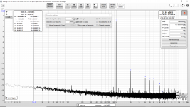
Perhaps worth adding the loopback response (the measurement rig, but not the DUT amp) to provide some perspective as to your benchmark noise/harmonic levels.
First attached is Left TRS to B XLR which gives us an idea of what the ADC side is capable of. (The balanced attenuator connects to the B XLR bypassing the NE5532.)
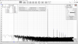
Second attached Left TS to B TS which shows the cleanliness (or lack of in terms of generator/DAC harmonics and power line harmonics) that will go into the power amplifier input. (But the NE5532 is there.)
The E-MU 0404 USB interface is powered by battery bank.
Second attached Left TS to B TS which shows the cleanliness (or lack of in terms of generator/DAC harmonics and power line harmonics) that will go into the power amplifier input. (But the NE5532 is there.)
The E-MU 0404 USB interface is powered by battery bank.
Attachments
Last edited:
- Home
- Design & Build
- Software Tools
- How to - Distortion Measurements with REW