Your plots certainly look much cleaner with the increased resolution.Here the improved (according to your recommendations) clearer graph containing results of these two simulations:
I had a look at your .asc file and stepped Vspread 0.60-0.72 with Vin -10 to 10V:I read some really negative opinions about some of the models released by onsemi over a decade ago. It seems they haven't updated anything since then - the same files are still hanging on their site.

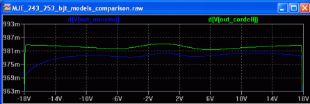
At first sight, the onsemi plot looks decidedly weird, and still doesn't look right if we normalise the y-axes:

I don't trust the plots using the OnSemi models and think you're right to stick to Cordell's models. I am going to make a wild guess that OnSemi optimised their spice model for driving a loudspeaker, because if you make Re=0.22 and Rload 8R, you get the following plots:

I think you need to repost your question in Headphone Systems or Solid State Amplifiers for an answer to questions like this!If you think about it, choosing a side driven through the bias spreader with non-zero impedance can increase or decrease distortion. It may turn out that closer to the ideal cfp vbe multiplier will give a worse result than a simple circuit based on one transistor or a series of diodes.😀
It's not a big deal but would be interested to know what trend these components actually exhibit and why it happens. I would guess that the hfe itself has rather little to say here, so is it related to the base resistance or perhaps one of the parameters responsible for beta droop?
Audio Potentiometer
I had a go at interpreting the information on LTwiki on potentiometer spice models. I started out with Mary West's video on including a linear potentiometer in a circuit then moved on to H Sennewalds models on LTwiki. I was just fumbling around but came up with something which appears to act like an audio pot. I attempted to follow the model for a cheap commercial pot as that is what I have in reality. An aliexpress version of an 250k Alps audio pot. Would appreciate any help to fix bugs and make it better. Zipped file attached.
I had a go at interpreting the information on LTwiki on potentiometer spice models. I started out with Mary West's video on including a linear potentiometer in a circuit then moved on to H Sennewalds models on LTwiki. I was just fumbling around but came up with something which appears to act like an audio pot. I attempted to follow the model for a cheap commercial pot as that is what I have in reality. An aliexpress version of an 250k Alps audio pot. Would appreciate any help to fix bugs and make it better. Zipped file attached.
Attachments
Hi RW988,...It's not a big deal but would be interested to know what trend these components actually exhibit and why it happens. I would guess that the hfe itself has rather little to say here, so is it related to the base resistance or perhaps one of the parameters responsible for beta droop?
I had a look at the models and the OnSemi model has a very low Early parameter (VAF), otherwise they are similar. The low Early effect parameter causes the gain to droop at higher input voltages as well as lowering the average gain.
A low VAF Early value may be due to testing with slower pulse times where internal heating causes the curves to flatten ( and if way too slow they can show a negative dynamic conductance).
Bear in mind SPICE models are isothermal -- they show only a snap-shot or freeze-fame of what happens in a real amplifier -- in a real amplifier the junction temperatures varies semi-randomly with music levels.
With junction temperature changes by more than a few degrees, like they do, you can't expect to keep your bias at an optimum level when listening to music. It is unfortunate but we can't sense the junction temperature accurately in real time to do much about it. That's why we need to use so much negative feedback to keep distortion low enough when the curves change from optimum to non-optimum. Other than that, using minimal emitter resistance which increases the optimum bias current which increases idle dissipation which is helpful to reduce temperature variations as well as widening the Class-A crossover region so you don't need to use so much feedback to make life easier for yourself as a designer.
Re: HFE variations.
In a simple output stage like you simulated where the input voltage has no source resistance you have pure voltage drive and this means base currents do not significantly affect the wingspread curves - the curves are mainly from the IS parameter (the Schotky equation exponential proportionality constant).
If there is some variation in the HFE with current (using param IKF) then this parameter also modulates the IS parameter and hence the wingspread plots are affected indirectly...
OR
If there is some variation in the internal base resistor with current (params RBM and IRB) then there is a secondary effect on the wingspread plots with pure voltage drive. Effectively, a nonlinear base resistor adds a nonlinear component to the external emitter resistance.
Attachments
Last edited:
Haha, the trend is reversing and pnp is starting to dominate here too. Surprise 🙂 Your guess may be right. If I remember correctly, the use of mje243 as driver or Vas was what gave the biggest discrepancies in simulation results.I am going to make a wild guess that OnSemi optimised their spice model for driving a loudspeaker, because if you make Re=0.22 and Rload 8R, you get the following plots:
The manufacturer writes: These devices are designed for low power audio amplifier and low−current, high−speed switching applications. But, as I see it, most of the diaudio community uses these transistors for much lighter tasks 🙂
Right, I will think about it. I'm not going to use it to drive headphones, but indeed the load impedance is quite similar 🙂 Thanks!I think you need to repost your question in Headphone Systems or Solid State Amplifiers for an answer to questions like this!
Wow, so it turns out that the factory measurement conditions itself changed results? This completely changes my perspective on the matter. I have always thought that factory models are developed to provide a reasonable compromise in simulation accuracy over the widest variety of intended applications.I had a look at the models and the OnSemi model has a very low Early parameter (VAF), otherwise they are similar. The low Early effect parameter causes the gain to droop at higher input voltages as well as lowering the average gain.
A low VAF Early value may be due to testing with slower pulse times where internal heating causes the curves to flatten ( and if way too slow they can show a negative dynamic conductance).
I am planning to use NF-loop. It is just a current supporter for the opamp driving a slightly heavier load. Although of course I don't want to rely only on the negative feedback, so some initial linearity should be maintained. I also don't want to force these transistors to work at their limits to avoid sacrificing reliability. I have looked at some quite similar application examples and for the MJE243/253 pair at comparable or lower RL there is a tendency to use RE rather larger than 2R2. This even satisfies me, because with some 9-12mA idle current and voltage swing reaching the supply rails these transistors still operates in SOA for DC and at TA=25*C without heatsink(I will put some small heatsinks on too of course). Do you have any suggestions how much RE can be safely reduced?Bear in mind SPICE models are isothermal -- they show only a snap-shot or freeze-fame of what happens in a real amplifier -- in a real amplifier the junction temperatures varies semi-randomly with music levels.
With junction temperature changes by more than a few degrees, like they do, you can't expect to keep your bias at an optimum level when listening to music. It is unfortunate but we can't sense the junction temperature accurately in real time to do much about it. That's why we need to use so much negative feedback to keep distortion low enough when the curves change from optimum to non-optimum. Other than that, using minimal emitter resistance which increases the optimum bias current which increases idle dissipation which is helpful to reduce temperature variations as well as widening the Class-A crossover region so you don't need to use so much feedback to make life easier for yourself as a designer.
Thanks for this clear explanation. I'll review again the parameters in these models and maybe I'll finally understand something more from it. 🙂Re: HFE variations.
In a simple output stage like you simulated where the input voltage has no source resistance you have pure voltage drive and this means base currents do not significantly affect the wingspread curves - the curves are mainly from the IS parameter (the Schotky equation exponential proportionality constant).
If there is some variation in the HFE with current (using param IKF) then this parameter also modulates the IS parameter and hence the wingspread plots are affected indirectly...
OR
If there is some variation in the internal base resistor with current (params RBM and IRB) then there is a secondary effect on the wingspread plots with pure voltage drive. Effectively, a nonlinear base resistor adds a nonlinear component to the external emitter resistance.
I realize that the source resistance while quite low is not zero (the loop closes at the output). But it's hard to take any specific value, because opamp's open-loop impedance is frequency dependent, so I'll deal with the influence of this parameter on linearity later.
Does anyone know how LTSpice is implemented? Is it able to take advantage of muli-core processors?
I'm trying to decide between a many-core processor and a fewer-cores but faster processor. And does the amount of L1 cache make a major difference in performance?
I'm trying to decide between a many-core processor and a fewer-cores but faster processor. And does the amount of L1 cache make a major difference in performance?
Hi RW988,...I am planning to use NF-loop. It is just a current supporter for the opamp driving a slightly heavier load. Although of course I don't want to rely only on the negative feedback, so some initial linearity should be maintained...
One way to make the power stage biasing fairly stable is to cascode the power stage. EG using another pair of the same transistors and biased LED's to offset the cascode bases. I haven't used this so I can't offer a buildable circuit but can help you develop one if interested.
Another option that I have built is current driven power transistors like used in this recent post What causes BJT based amplifier distortion? but my circuit was for a 100W amp published in Linear Audio Apr 2017 (Vol.13) and some comments recently posted here What causes BJT based amplifier distortion? You can scale my circuit down to make a good headphone amp. And you don't need any feedback around the output stage for a headphone amp and the output stage will be short-circuit proof if the voltage to the power stage driver is clipped.
Yet another option is my India topology here Has anyone seen Rush pairs used this way? Post 1 is for a power amp that does not use any feedback and provides inherent current drive to the speakers or headphones and has voltage gain.
At first the "India" topology looked like a variant of the circlotron topology, but on later inspection I decided it was a bridged topology (also called balanced topology these days). So far I have bench tested it and someone has tested a PCB version for commercial use (Not shown in the link is the Vbe multiplier for bias stability.).
BTW it has inherent speaker/headphone DC protection. The downside (at least for DIY) is the inconvenience for two secondaries for each channel which equates to one standard transformer for each channel.
LTspice uses multicore processors, but does so rarely. For example, a quad-core speeds up the count by a factor of three. LTspice decides by itself whether to connect additional cores to the calculation. LTspice does this when the electronic circuitry is large enough. Most electronic circuits do not use multi-core.
I go look.
Update, I did look at it and understand it, on model in thread pinnumbers are used but I have names, but result is the same.
Thanks.
Update, I did look at it and understand it, on model in thread pinnumbers are used but I have names, but result is the same.
Thanks.
Attachments
Last edited:
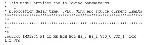
This is a good use of LTspice's symbol auto-generation feature, since there is no built-in symbol for the LMG1205. Attached is a ZIP file containing the auto-generated symbol using the technique described in the link below:
LTspice: Simple Steps to Import Third-Party Models | Analog Devices
Note that according to the datasheet, VDD_0 and VDD_1 are connected together internally, as are HS_0 and HS_1. The subcircuit represents these connections via a 1 milliohm resistor. I gather from the application notes that you can make your external connection to either one of these pairs of pins, which are labeled VDD and HS on the pin-out diagram. So an alternate symbol is included in the ZIP file that has only 10 external pins, with each pair replaced by a single pin, labeled VDD and HS respectively. One member of each pair has its label removed, but is still included in the symbol file. This alternate symbol more-or-less matches the arrangement shown in the "Simplified Application Diagram" on the first page of the datasheet.
Disclaimer: I haven't tried this symbol so use at your own risk.
Attachments
Thank you very much Ray, You did make mine day. And it is already nice here, we have in february 19 degrees and tomorrow even 20, normal is 6..
I had read the advises, I did see that it has no schematic into it like the other had and as such did have to find that out, but you did help approchiate it very much.
The connections with the 1 milliohm resistors are pins on the ic who is on two sides, for better earthing and vcc connections. WE talk abouw Gan driver who are very speedy.
regards and have a nice day.
Last edited:
I'm glad to help, and I hope that one of these symbols will work for you.
One note on the alternate symbol: The unlabeled pins show as rectangles inside the box and these cannot be removed from the symbol or else LTspice will report a pin mismatch between the symbol and the subcircuit. This is because the subcircuit contains 12 definitions in its pin order so the symbol must also have 12 pins, in the same order, whether they all have visible labels or not.
Good luck.
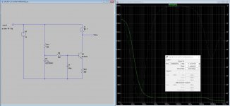
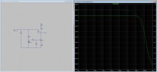
I am used to simulate the output impedance of an amplifier using the current source (1A) method with good results.
I am now trying to do the same with a one bjt CCS where I want to determine the output impedance but the results are not what I expected.
In this case I am getting a reading of 11ohms at 1khz and I believe something is wrong with my sim.
I am sure this has already been discussed here but this thread is really long and I did not find the needed info.
Please guide me in the good direction.
Attachments
It looks to me there is no DC standing current in the BJT you are measuring? I always look at the waveform at the test point with a .tran to make sure all is OK, and I don't overdrive the circuit with my test current.
Make sure that the standing DC current is at least as large as thge peak test current. Testing with a 1A current source is a bit high, that would mean your stage needs at least 1A DC standing current.
Jan
Make sure that the standing DC current is at least as large as thge peak test current. Testing with a 1A current source is a bit high, that would mean your stage needs at least 1A DC standing current.
Jan
Last edited:
Make sure that the stage you test works as it should without the test current source. That all its DC conditions are OK. Then use a test current that is lower than the DC current at the point you are testing, and couple the test current in through a cap to avoid upsetting the stage you are measuring.
Most of these conditions are met with a usual class A or B audio amp, but with a single ended stage you need to take care of that.
Jan
Most of these conditions are met with a usual class A or B audio amp, but with a single ended stage you need to take care of that.
Jan
- Home
- Design & Build
- Software Tools
- Installing and using LTspice IV (now including LTXVII), From beginner to advanced