You have made me laugh we the "characteristics" that rabid audiophiles require! Really I'd call that a desease!")
+1
My F6 is finally up and running. And sounding way better than it has a right to after such a short break-in period.
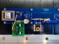
Why am I posting this here in the M2x thread? Because I created a challenge for myself by extending the design parameters of the amp to the point that it needed a different input buffer. Based on experience with my M2x, I chose to use a variation of the Diamond buffer, basically a tweaked Austin input stage. In order to run safely at +/– 26.4 V, I designed the output stage around a pair of Toshiba TTC004B and TTA004B bipolar drivers. Their TO-126 package is somewhat more thermally efficient than the E-line package of the ZTX parts used in Austin. I added 10 Ohm base resistors and used 10 Ohm emitter resistors on those devices, and haven't found it necessary to add heat sinks.
Remarkably enough, it all fits on a Vero board that is the same size as the Austin PCB. Eliminating the M3 mounting hole pads frees up some space. The keen observers may notice a couple other changes as well. Once I've taken a couple more pictures and possibly made some measurements, I will post a proper write-up in the appropriate F6 thread. But for now I want to thank MJ and 6L6 for making the M2x, and this extension of the F6 possible.
Attachments
Last edited:
My F6 is finally up and running.
Beautiful job!
Well done.
Always interested in assemblies on strip board, that's how I do 95% of my projects.
Looking forward to your unbiased comparison of F6 and ACA Premium.
(I know it's not fair but still...)
Socketed the first stage BJTs (2 x (EF + CS)) but not the second? Possibly because the second stage's TO-126 package pins are fatter than socket holes and, unmodified, are on a pitch of 0.085" rather than 0.100" like the stripboard and socket?
The LM4040 ICs are also housed in three-lead transistor packages, but unsocketed.
Omitting the pole-zero compensator might change the response to fast risetime square waves, using those Toshiba devices. Either for the better or the worse. NP and I went back and forth on this question a couple times in early 2018.
_
Attachments
Last edited:
Hi Mark. Yes, the socketed devices are as you have depicted in your schematic. When I installed the LM4040 ICs, I removed the unused leg and soldered them directly into the board. The TO-126 packages don't socket well into veroboard, so those were also soldered directly.
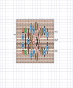
It is somewhat obvious that the photo and the vero layout drawing don't match each other. The photo was of the first implementation, an incorrect one that caused four resistors to be sacrificed in the name of science during the first channel board smoke test. The vero layout drawing shows the boards as currently built, where it was necessary to use insulated wire for the two power jumpers. It would be possible to un-cross those wires in a new layout, but that would require a different set of trace breaks. I decided I liked the look of the crossed wires, as they reminded me of the important power connections.
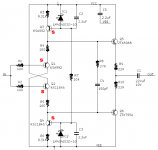
I did a little online research about diamond buffers before choosing to go with this one. I did run across some versions that used small value capacitors between the base pins of the output transistors to counteract a minority-carrier anomaly which showed up in high slew-rate square waves. (I believe whoop-de-do is the technical term.) Yours is the only one I've seen so far with an RC network. I simply reverted to an earlier practice of mine to install base resistors in front of drivers to control linearity and bandwidth. The 10 Ohm value is a placeholder for now, until I determine if another is more appropriate.
It is somewhat obvious that the photo and the vero layout drawing don't match each other. The photo was of the first implementation, an incorrect one that caused four resistors to be sacrificed in the name of science during the first channel board smoke test. The vero layout drawing shows the boards as currently built, where it was necessary to use insulated wire for the two power jumpers. It would be possible to un-cross those wires in a new layout, but that would require a different set of trace breaks. I decided I liked the look of the crossed wires, as they reminded me of the important power connections.
I did a little online research about diamond buffers before choosing to go with this one. I did run across some versions that used small value capacitors between the base pins of the output transistors to counteract a minority-carrier anomaly which showed up in high slew-rate square waves. (I believe whoop-de-do is the technical term.) Yours is the only one I've seen so far with an RC network. I simply reverted to an earlier practice of mine to install base resistors in front of drivers to control linearity and bandwidth. The 10 Ohm value is a placeholder for now, until I determine if another is more appropriate.
Last edited:
Question on the transformer:
Mark has mentioned that he used a 300VA transformer with dual 18v secondaries.
Question is: I have couple of 300VA transformers with dual 22v secondaries and can I use them on M2X. They are the Antek AS-3222 transformers. If not then I would order a 300VA with 18v secondaries from Antek.
Thanks!
Mark has mentioned that he used a 300VA transformer with dual 18v secondaries.
Question is: I have couple of 300VA transformers with dual 22v secondaries and can I use them on M2X. They are the Antek AS-3222 transformers. If not then I would order a 300VA with 18v secondaries from Antek.
Thanks!
If you use a classic power supply, the transformer is too large. I saw here on forum an alternative power supply project (SLB?). 2x22v will probably be good for that
I also saw the SLB power supply, will give it a try. Its limited to 3+ amps (or atleast tested with load).
I am going to be mounting this in a 4U deluxe chassis, so that I can try out different amps.
I would suspect that 18VAC secondaries are a good match to 3U height full depth heatsinks.
While 4U height full depth heatsinks are a good match to 18 * (4/3) = 24VAC secondaries.
what about the square root? Not applicable here since the bias current is constant. P=V*I = V*constant
While 4U height full depth heatsinks are a good match to 18 * (4/3) = 24VAC secondaries.
what about the square root? Not applicable here since the bias current is constant. P=V*I = V*constant
I’m using a pair of Antek AS-3222 transformers with SLB power supplies in my F6. I used a different set of transistors in the CFP, which reduced the dropout voltage from 3 Volts to 2.1 Volts. The output voltage of each supply is +/– 26.4 Volts while providing 1.4 Amps to the channel board. The nature of of the SLB as a “ripple eater” makes the final output voltage somewhat difficult to pin down. A single SLB powering a typical M2x might end up at 25 Volts. This is at the upper limit of some of the canonical input stages that come with the M2x PCB set.
That’s a long way of saying it would be easier to build a more conventional supply using a transformer with 18V secondaries. Unless you’re willing to modify the input stages and/or the SLB so they are compatible with each other.
That’s a long way of saying it would be easier to build a more conventional supply using a transformer with 18V secondaries. Unless you’re willing to modify the input stages and/or the SLB so they are compatible with each other.
Subbu,
Good to see you at the Pass Labs forum and wishing you a fun build with your M2X. The folks on the forum are very helpful, keep us posted on your progress.
Just an observation - if you are opting for an Antek transformer, please check the specs - most of them show some "sag" under load. For reducing the sag, you might want to opt for a 400VA unit if choosing Antek. Another option is go for a 2 x 20V AC, 300 VA transformer from Antek, so even after the sag after load, you should be good for 24-25 VDC on the rails.
The transformers are designed for 120VAC mains - if your mains is lower, then you will have lower output at the secondaries. Maybe you can check?
Good to see you at the Pass Labs forum and wishing you a fun build with your M2X.
The folks on the forum are very helpful, keep us posted on your progress.Just an observation - if you are opting for an Antek transformer, please check the specs - most of them show some "sag" under load. For reducing the sag, you might want to opt for a 400VA unit if choosing Antek. Another option is go for a 2 x 20V AC, 300 VA transformer from Antek, so even after the sag after load, you should be good for 24-25 VDC on the rails.
The transformers are designed for 120VAC mains - if your mains is lower, then you will have lower output at the secondaries. Maybe you can check?
A quick update on the performance of the diamond buffer as an input stage for my F6..
After changing the connection of the upper bias caps (C1) on my F6 boards, and confirming lower distortion levels, I finally got around to looking at some square waves on my scope. Rising and falling edges are very fast and clean, with no apparent minority carrier anomalies. The top and bottom edges of the square wave do exhibit a significant amount of ringing, however. Looks like it's time to switch the output emitter resistors to 22 Ohms, as specified in the Austin schematic.
Regarding the power supplies, I will also be adding some large bulk caps (24 mF, 40V) to the outputs. There is some indication that this may prove beneficial. Twenty Hz sine waves look fine, but the 1 kHz square waves were jumping around a bit. This wouldn't be the first time I've seen an improvement to the performance of a CFP capacitance multiplier by adding a large value cap on the output.
Thanks, I got the cabinet from China and here is the link to the VU meters. 2PCS hifi Amplifier VU meter DB level Header Lamp indicator Peak+1PC Drive board-in Amplifier from Consumer Electronics on Aliexpress.com | Alibaba Group
Instead of watts they measure "WATIS"
Put input and output on a dual trace scope and display both. Some or all of the ringing might be present on the trace of the input, suggesting that either the wave generator's output is imperfect OR that the test fixturing is adding a bit of L*dI/dt to the traces.The top and bottom edges of the square wave do exhibit a significant amount of ringing, however
It's true that I don't often use square waves as a test signal. My signal generator is EE Toolkit Pro running on an iPad Mini. My measurements were at the output of the buffer and the output of the amp. They tracked each other quite well, accounting for gain of the amp. Worth checking the signal at the RCAs, as well as confirming the probe compensation.
The amp is already partially disassembled, so will double check test bed integrity once it's back together with the new resistors.
The amp is already partially disassembled, so will double check test bed integrity once it's back together with the new resistors.
Sure enough, it was a case of Garbage In -> Garbage Out. Hmmm. At least I did the test before swapping any resistors.
Anyway, the input buffer and amp do a really good job of replicating the less than perfect square waves coming from my various phones and tablets. Maybe it's time to fab a super-special 1/8" phono to stereo RCA cable. I think I have some old RCA terminated video cable around somewhere...
Anyway, the input buffer and amp do a really good job of replicating the less than perfect square waves coming from my various phones and tablets. Maybe it's time to fab a super-special 1/8" phono to stereo RCA cable. I think I have some old RCA terminated video cable around somewhere...
Last edited:
I use BNC connectors to get low-inductance grounds for inputs and outputs when doing 3ns risetime square wave testing. This picture is from post #439 in this thread. Signal generator input on the left, Oscilloscope output on the right.
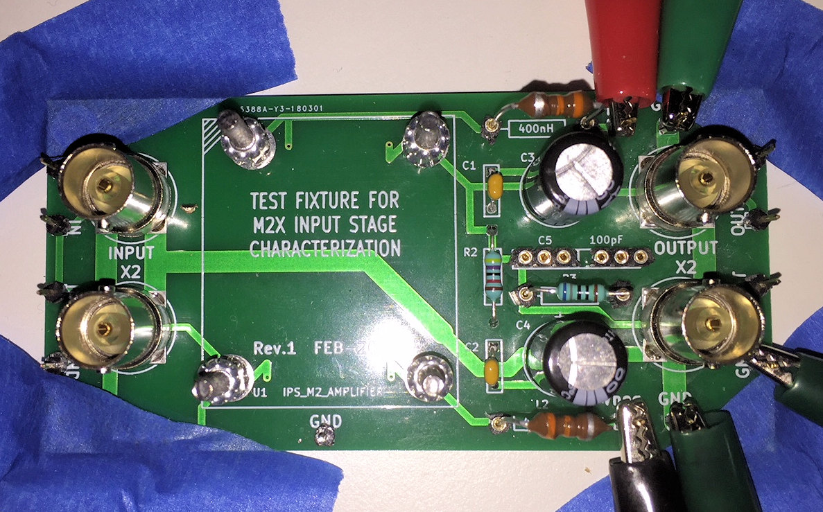
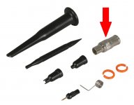
I install scope probe adapters that turn the probe into a coaxial plug whits fits perfectly into the BNC jack.
I install scope probe adapters that turn the probe into a coaxial plug whits fits perfectly into the BNC jack.
Attachments
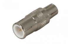
Most of the daughter card circuits are not able to drive a 50 ohm load; they're designed to drive the 600 ohm primary of the Edcor transformer. And if you omitted the terminator(s) on the BNC cable, reflections would ruin the nice free-of-ringing edges you're trying so hard to display.
- Home
- Amplifiers
- Pass Labs
- The diyAudio First Watt M2x