Did you cap the rails of the PCB? My God, suddenly bass is awesome. And not even on par with spec capacitance yet. Traveling towards bliss slowly and sloppyWhen I powered up and gave a listen, my first thought… “where did the bass go?”
I was impatient and used a 24V wallwart.
Good Gemini will be next")
Guess PSU inductance plays a role here. Loaded the regs too. Thank you, Pico!
I ordered the two boards that I drew up, the cap version and the no-cap version. I should have them within the next couple of weeks. I have made a few changes since the previous Gerbers that I posted like spreading the JFET holes apart to make them easier to solder as well all the changes suggested by Pico.
Once all is good and tested, I will go ahead and post them here.
Once all is good and tested, I will go ahead and post them here.
Not much. The difference between the original (I believe Nisbeth's is the original) and the no cap version I drew up is that there are a couple locations for resistors that you can use to bypass and jumper out the cap. So what you would do is measure both sides of the pot (one leg to center, then the other) after you set the DC offset, then place resistors that closely match these values.
What would be cool to try is to measure the difference and see if you can get it down to a lower value or maybe even one resistor. For instance, using a 50 ohm pot, if you had say, 20 and 30, maybe try a 10 ohm on the 30 side, no resistor on the other. Just a little extra tweaking capability.
So you would solder a jumper where the pot goes and just tack it down to the middle pad with a bit of solder. This of course after bypassing the pot etc. If you have close enough matched JFETS and have virtually no DC offset, then you can jump all three locations.
Attachments
That I don't remember. Load the the previous Gerber's into JLCPCB. That should show you the size
Like I said up above, I spread The JFET pads apart to make soldering easier. So if you want to order the PCBs before I get them and test them a little bit, I can PM you the Gerber.
I plan to post it here after I confirm everything's all good.
One thing that would be cool for the cap version would be a jumper that could be removed to take the caps out of the circuit
This is it. I have the same one. It is a nice little power supply. I use it on a BA2018 and it works very well and has been very reliable. I keep hearing the word shunt thrown around so maybe see how that goes.
https://www.audiosy.net/2021/01/21/meet-helios-bi-polar-power-supply-rev-b-boards-coming-soon/
https://www.audiosy.net/2021/01/21/meet-helios-bi-polar-power-supply-rev-b-boards-coming-soon/

You sure that’s not just your neighbours yelling for you to stuff it/turn the volume down?I keep hearing the word shunt thrown around so maybe see how that goes.

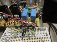
I was gonna wait for a pcb but decided to go proto board, since it such an easy circuit. Haven’t had a chance to listen to it yet, but vitals all seem good. +-12V on the nose (voltage divided down from +-28V, with 470R and 470R).
I didn’t have a pot but had some 24R resistors for the degenerates. One channel is around 6mV offset and the other 2mV. Will test out and report back!
I didn’t have a pot but had some 24R resistors for the degenerates. One channel is around 6mV offset and the other 2mV. Will test out and report back!
Attachments
Last edited:
Tested this out today. Works perfectly! I had a tube stage going into a 100k stepped attenuator going into a 47k solid state power amp. The attenuator was not functioning correctly because of the mismatch. This definitely cured it. Will do some more relaxed listening tests today. So far just tested it out briefly and looking at on the scope.
Doesn’t get any simpler than this folks!
1ma offset on each channel. I adjusted by putting a 200ohm resistor in parallel with the lower 24ohm resistor. +1 mv on one channel and -1mv on the other. Close enough! Time to get a beer and listen as zen mod would say. Although it’s just 6am on a Sunday lol

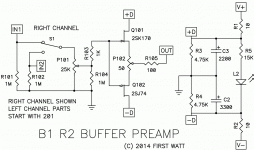
Okay so I tried the No-cap version of the B1 R2 board that I drew up. I made a few changes after trying the boards.
Here are the changes that I made:
-Spaced JFET pads apart and made them much larger. Much easier to solder.
-Made resistor locations where you may use jumpers have larger pads to make it easier to solder/desolder them
-Made input and output holes larger. If using the terminal block, you'll have to hold it straight due to the larger holes. I like to solder wires in so I made the holes larger for that reason.
-I added a couple jumper locations for + and - for a mono power supply. That way you don't have to run wires to jump accross to the other channel.
-Added a GND Jumper up by the signal side for GND which is also neg input/output.
I used the footprint from this part for the input and output connectors. I didn't test the part.
https://www.digikey.com/en/products/detail/molex/0393570002/946543
I put the boards together with some cheap carbon comp resistors to test and it worked well. The matched JFETs had 0.3mv on one channel, -0.1 on the other. Hooking it up to my amp, I had 7.1mv with the preamp not connected, and 9.1 with it connected using the 0.3mv offset channel of the B1 R2'ish. It sounded nice. I zip-tied the JFETs together and couldn't really get the offset to budge by touching one or the other. Pretty stable. I didn't test the buffer hooked up to the amp turning it on or with the preamp off.
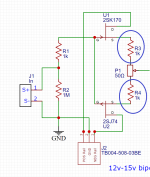
So use a 12v-15v bipolar supply, attached is the gerber file which uploads right into JLCPCB.
I will make the same alterations within the next couple of days to the capacitor version of this board.


Here are the changes that I made:
-Spaced JFET pads apart and made them much larger. Much easier to solder.
-Made resistor locations where you may use jumpers have larger pads to make it easier to solder/desolder them
-Made input and output holes larger. If using the terminal block, you'll have to hold it straight due to the larger holes. I like to solder wires in so I made the holes larger for that reason.
-I added a couple jumper locations for + and - for a mono power supply. That way you don't have to run wires to jump accross to the other channel.
-Added a GND Jumper up by the signal side for GND which is also neg input/output.
I used the footprint from this part for the input and output connectors. I didn't test the part.
https://www.digikey.com/en/products/detail/molex/0393570002/946543
I put the boards together with some cheap carbon comp resistors to test and it worked well. The matched JFETs had 0.3mv on one channel, -0.1 on the other. Hooking it up to my amp, I had 7.1mv with the preamp not connected, and 9.1 with it connected using the 0.3mv offset channel of the B1 R2'ish. It sounded nice. I zip-tied the JFETs together and couldn't really get the offset to budge by touching one or the other. Pretty stable. I didn't test the buffer hooked up to the amp turning it on or with the preamp off.
So use a 12v-15v bipolar supply, attached is the gerber file which uploads right into JLCPCB.
I will make the same alterations within the next couple of days to the capacitor version of this board.
Attachments
Last edited:
- Home
- Amplifiers
- Pass Labs
- B1 Rev. 2