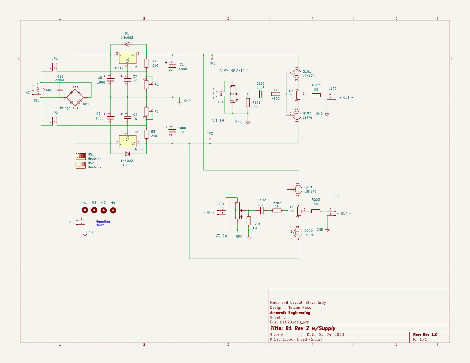
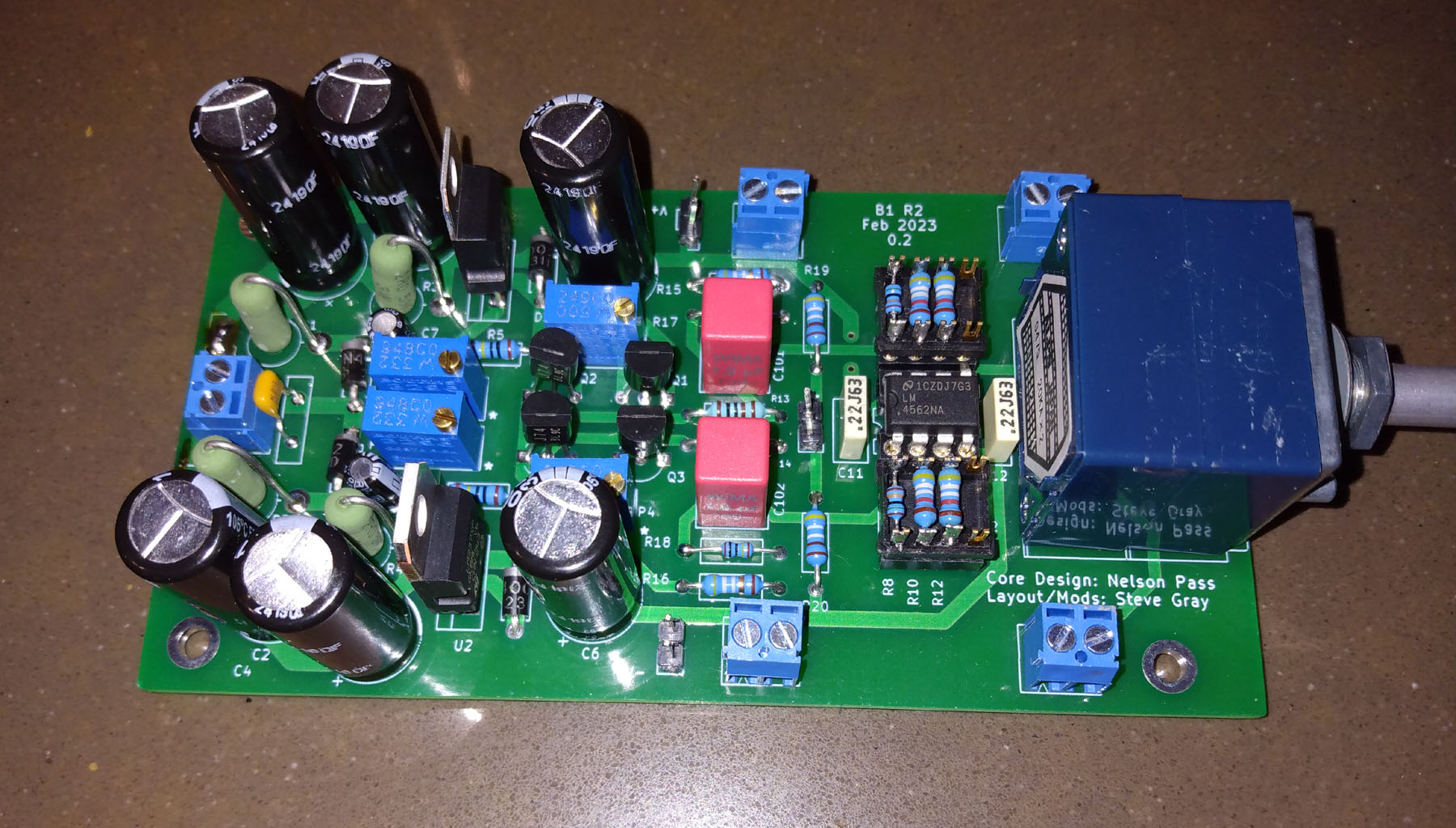
I'm doing the stupid dance right now. I'm almost done and realized it should be better AND I made a mistake. So a little rework is needed before it's turned on.I got these boards back last week. I saw some one else do something similar and wanted one for myself so laid out my own. I may be able to get them stuffed and tested this weekend. It uses LM317 and LM337 for the regulators and an Alps pot. I'll use a wall wart transformer. There are also jumpers so you can forgo the onboard power supply and populate and use it with an external supply. The pot is sitting on the board to show scale.
If it works Ok, I'd be happy to share the boards, BOM, Gerbers, or KiCad project files.
1) My dremel will help isolate the filter cap grounds so they can be wired directly back to the main ground point to keep spike current out of the signal ground plane.
2) I used a library footprint for the diode bridge and discovered the pinout is wrong!!! So I'll have to find a different t bridge part or wire a kludge. It seems the part I have is wired + ~ ~ - and the footprint I used was ~+~- :-(
3) I'm also going to add a 0.1 uF cap between the ground plane and chassis ground.
4) I'll also add a few ohms between AC source and the first filter cap to limit current spikes.
5) And last, calculations show that the heats sinks are completely unnecessary given the current draw of this circuit.
Maybe I will be able to turn it on next week. In the mean time I've laid out a new board with the improvements.
If you were concerned about needing a small heatsink, you could always just make enough room for these standing vertically. I use them every once in a while, I just snip off the little solder lead. Also, I am not seeing a reason for an insulator as there is only one device per heatsink right?
https://www.digikey.com/en/products/detail/assmann-wsw-components/V8508B/3476147
I agree though, the JFETs themselves do not even get warm. I doubt those TO-220 devices are going to see any heat.
https://www.digikey.com/en/products/detail/assmann-wsw-components/V8508B/3476147
I agree though, the JFETs themselves do not even get warm. I doubt those TO-220 devices are going to see any heat.
Hi all, looking for suggestions from the more experienced hive mind re my post #421 above.
I fixed my power supply issue and now have a rock solid +/- 12V supply.
I have also double checked all the connections, values and solder joints yet still have a problem.
I am using a 50 ohm balancing pot with 50 ohms after that for the output.
The FETs are a matched quad of 8-11 mA Idss Toshibas from the DIYAudio store.
It's a straightforward implementation of the original design with the possible exception of the high Idss FETs that should not be a problem.
I can zero out the offset when I first turn it on. But if I leave it sitting and come back after an hour or two the offset has drifted and cannot be adjusted back to 0. There are not enough turns in my multi turn pot, And this condition is identical for both channels.
Does anyone have any idea what is going on and how I can fix it. Do I have bad FETs? I must have done something ignorant.
Is C101/102 in the wrong place? I just realized there is infinite DC resistance from gate to ground. Could that be it?
Just for grins, here is the schematic. Thanks in advance for any tips.
I think that cap might be the problem. Charge can build on the gate and have no place to go. I'm gonna bypass the input cap it and see what happens. And I still welcome any and all opinions on this. Thanks!
Remove the input cap and jumper it and see what you get.
If that cap is bipolar it should be shunted to gnd. From a quick view of you circuit I see no other obvious explanation.
If that cap is bipolar it should be shunted to gnd. From a quick view of you circuit I see no other obvious explanation.
That did the trick. Now I need to connect it to something and see how it sounds!..... and also finish the rev 2 layout with corrections and improvements.
Thanks Papa! Well, it's not pretty. But it sure sounds good! Harmonic detail and imaging have kicked up a notch compared to the direct from DAC connection. And low end weight is better. I really did not expect anything this noticeable. This is a very pleasant development!!
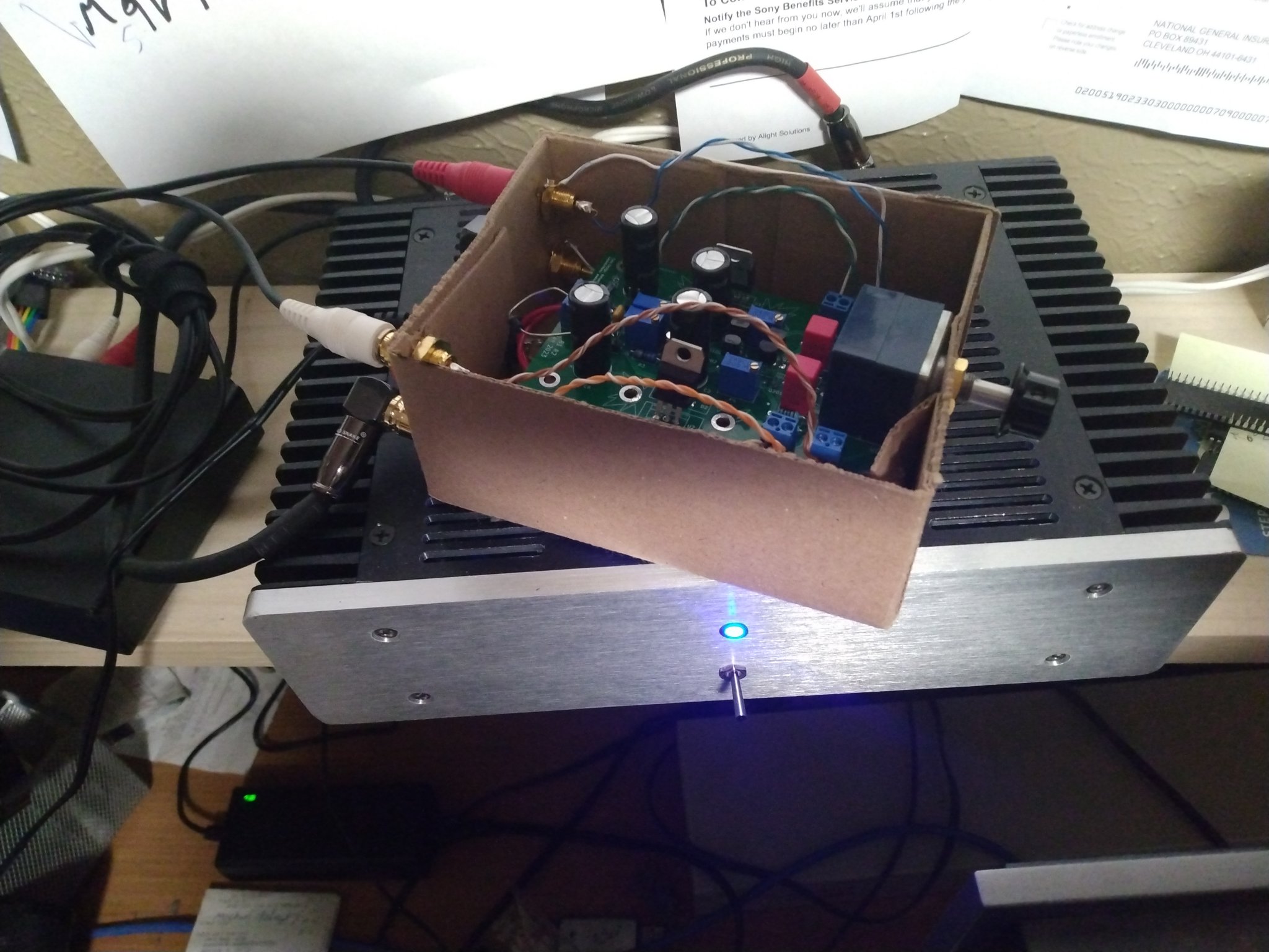
I had mistakes in my layout so a PS correction is blue wired, input caps are bypassed and regulator heats sinks are removed, Nothing wrong with the heat sinks, just unnecessary overkill.
I'm waiting for the real chassis to arrive. It should get here around the same time as the new boards and parts. The new board will also have RCRC input filters following the rectifier diodes. Yay!
I'm grooving on Little Feat as I write this. It's uncanny to hear complexity in Billy Payne's organ timbre that I never knew was there.
BTW, it's sitting on top of my custom conventionalized ACA Mini. What a great combination! Thanks again, Mr. Pass!
It just keeps getting better as I listen! Incredible! Nearfield office system. SDAC->B1R2->MiniACA-> sealed Markaudio CHR-70's. Is realism too overused a term? This is so good. I can't stop smiling!
The second revision was assembled today. I'll bring it up tomorrow. This one has the previous mistakes fixed, an improved power supply and an added configurable gain stage that can be completely bypassed if desired. There is no coupling cap before the gain stage. I hope that was not a mistake. But there is one before the output buffer. Or maybe I should put a jumper in to bypass that cap, too, and allow full DC operation? Decisions.

It works fine. Sounds good. But I'll bypass
the op amp and compare the sound w/o gain as well.
the op amp and compare the sound w/o gain as well.
The gain stage stays. It sounds great with or without it. I suspect Papa's output buffer is the final determiner of perceived sound quality.
I'm waiting for the chassis to be delivered now. I'll post a picture when it's all done. Now it's back to real work for me. :-(
I'm waiting for the chassis to be delivered now. I'll post a picture when it's all done. Now it's back to real work for me. :-(
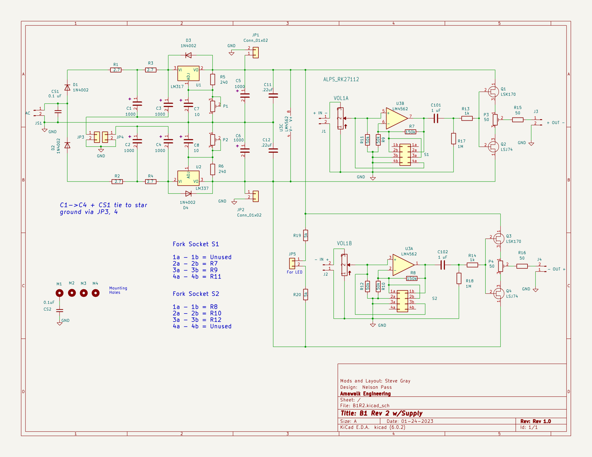
The schematic in #423 has been fixed. Below reflects the latest rev as built. The power supply is fixed and improved, the location of C1 now allows the FETs to bias properly and a configurable gain stage has been added. There is also a power LED connector and connectors to provide offboard V+ and -. But with no heatsinks on the regulators that must be used carefully if at all. Right now the regs are probably running no more than 10 to 20 above ambient.

Correction to above comment .....
There is also now a power LED connector. No external PS connectors. The funny jumpers by the AC in are just there to allow isolation of the ground path from the main smoothing caps. External PS is a 1A 24V wall transformer. Plenty of margin for a half rectifier with little load.
There is also now a power LED connector. No external PS connectors. The funny jumpers by the AC in are just there to allow isolation of the ground path from the main smoothing caps. External PS is a 1A 24V wall transformer. Plenty of margin for a half rectifier with little load.
Great implementation! I'm looking forward to your final assessment, especially when compared to the BA2018 (and any other preamps you have on hand).
Regards.
Regards.
- Home
- Amplifiers
- Pass Labs
- B1 Rev. 2