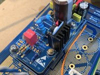
In retrospect, it's advisable to use M3 standoffs. They are slightly smaller diameter than 4-40. I looked VERY carefully and didn't see a problem, but the DMM doesn't lie. Or use Vunce's suggestion of some Kapton tape.
All is now good! Looks really great!! Super precision everywhere.
BK
Excellent progress BK!
Looking forward to your first listen 😀
Maybe nylon spacers and nylon washers would solve the problem without requiring meticulous visual inspection / electrical continuity testing?
9911-312 Bivar Inc. | Hardware, Fasteners, Accessories | DigiKey
9911-062 Bivar Inc. | Hardware, Fasteners, Accessories | DigiKey
9911-312 Bivar Inc. | Hardware, Fasteners, Accessories | DigiKey
9911-062 Bivar Inc. | Hardware, Fasteners, Accessories | DigiKey
Those would be ideal for chassis to PCB connection, but the daughter boards to mother board need electrical continuity.
or something like this:
https://www.amazon.de/Stück-rot-Iso...34&hvtargid=pla-349808521085&psc=1&th=1&psc=1
JP
https://www.amazon.de/Stück-rot-Iso...34&hvtargid=pla-349808521085&psc=1&th=1&psc=1
JP
The bolt provides electrical continuity from Mother to Daughter, while the insulating washer and/or spacer prevent inadvertent shorting from the bolt to adjacent copper traces on the motherboard.
If desired you could thread a normal, conductive metal, hex spacer onto the bolt after the insulating washer, which increases the electrical contact area between bolt and the bottom side of the daughterboard.
If desired you could thread a normal, conductive metal, hex spacer onto the bolt after the insulating washer, which increases the electrical contact area between bolt and the bottom side of the daughterboard.
The new Yarra with tented vias (solder mask covered) should prevent this sort of stuff in the future. It just shipped out today along with whole set of WBA18’s and PCA’s.
The tented via boards don’t have that gold bling look anymore - and the original exposed vias will now be a collectors’ item. 🙂 They do look pretty.
The tented via boards don’t have that gold bling look anymore - and the original exposed vias will now be a collectors’ item. 🙂 They do look pretty.
Hello builders,
to avoid every risk of short-circuit by mounting printed board assembly you could use following parts (here 10mm body length):
R30-6201014 Harwin | Mouser Deutschland
JP
to avoid every risk of short-circuit by mounting printed board assembly you could use following parts (here 10mm body length):
R30-6201014 Harwin | Mouser Deutschland
JP
Does anyone know what the pot boards fit? It looks like the smallest one is for the small ALPS and the big footprint for the large ALPS. Does the middle size footprint fit the TDK 2CP-601 Series?
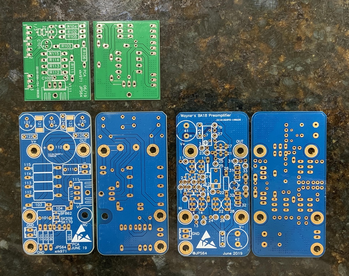
The PCBs are in: WBA18-Yarra, PCA-Yarra, PCA-Aksa Lender format.
Attachments
Last edited:
Hi Rick,
The pot board marked with R221 will fit the TKD 2CP-601 pot (2.5mm x 5mm centres)
The board marked with R201 will fit the Alps Blue Beauty type pot (5mm x 10mm centres)
The board marked with R211 will fit the smaller pots - various brands with 2.5mm x 2.5mm centres.
Regards,
Gary..
The pot board marked with R221 will fit the TKD 2CP-601 pot (2.5mm x 5mm centres)
The board marked with R201 will fit the Alps Blue Beauty type pot (5mm x 10mm centres)
The board marked with R211 will fit the smaller pots - various brands with 2.5mm x 2.5mm centres.
Regards,
Gary..

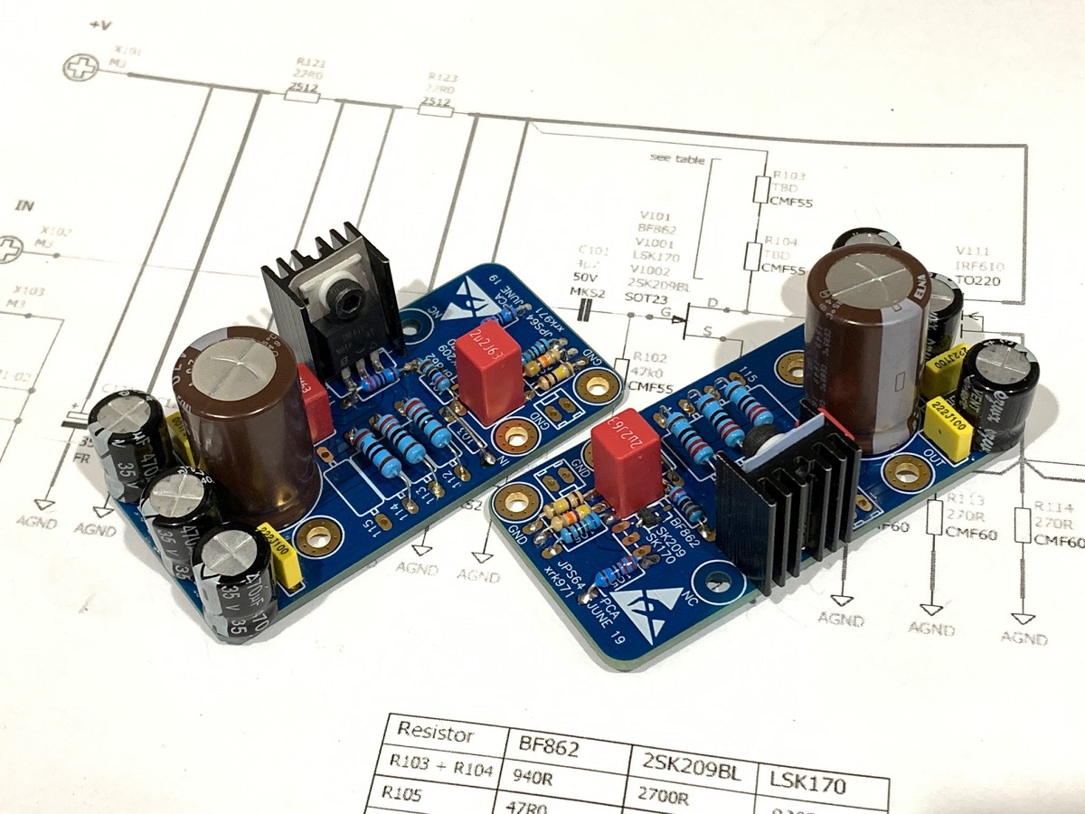
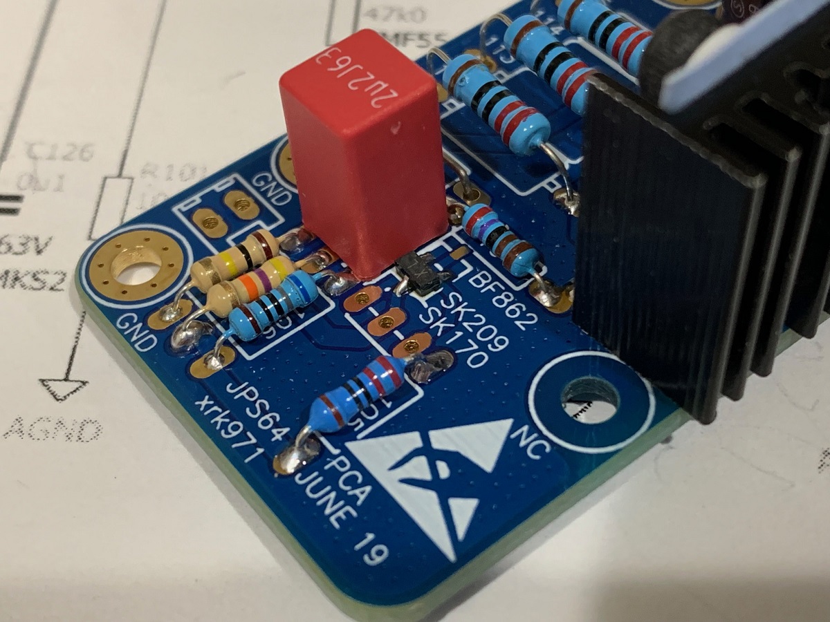
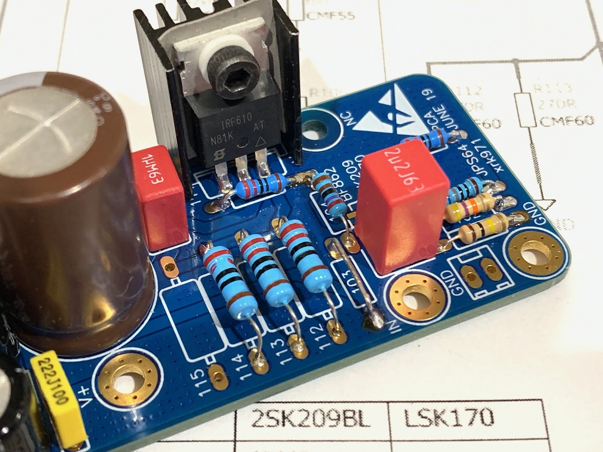
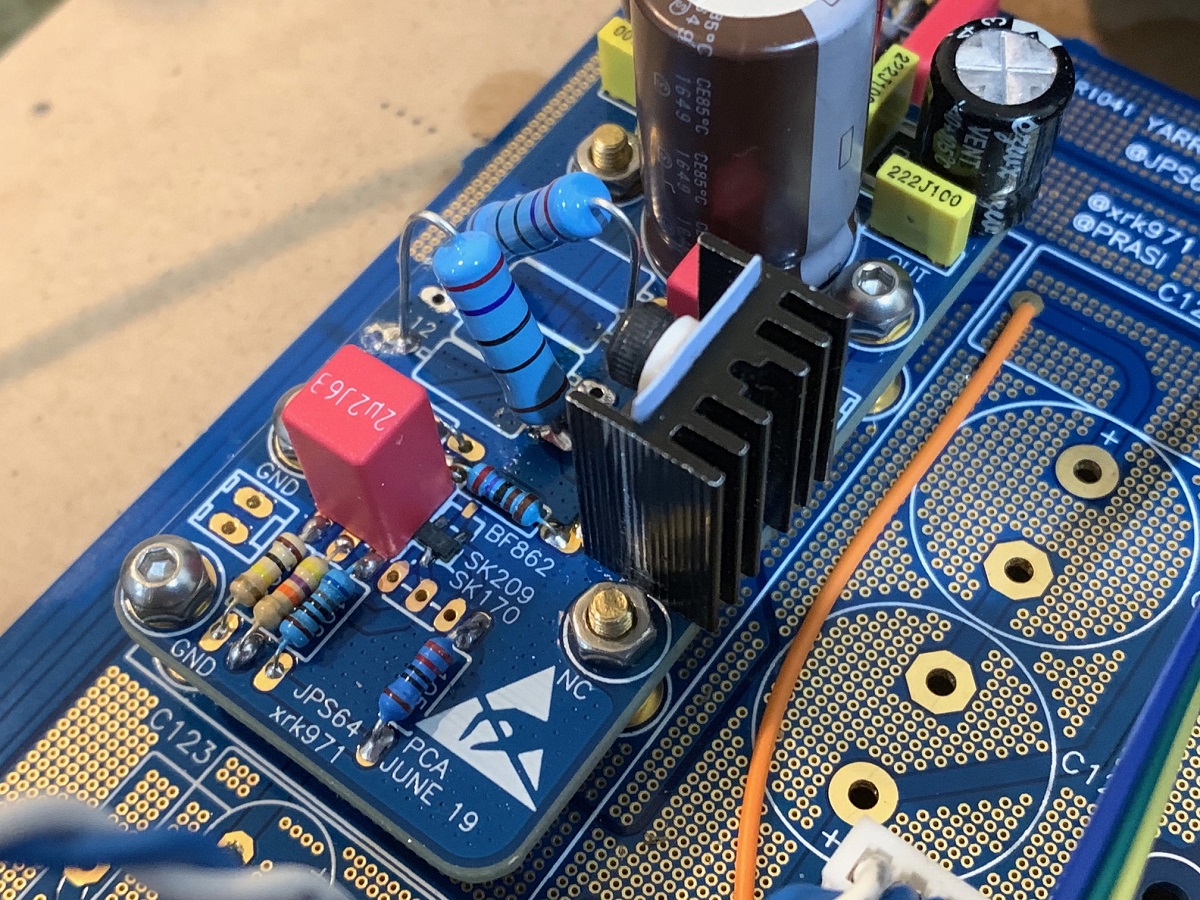
I just verified that the Yarra PCA daughterboards work. I used 2SK209's for the JFET. Using the values for the source resistors in the table resulted in a much too high of a current of 190mA and the resistors started to cook. I found that using a pair of 2W 270ohm resistors in parallel (for 135ohms net) gave 122mA bias current and a reasonable amount of heating (1W per resistor) with a Vcc of 27.5v upstream of the CRCRC. The 2SK209 can take a higher supply voltage than the BF862. Listening to the output on headphones, it sounds great. Just the sound I expected from the PCA. The output noise measured with Fluke 101 was 0.0mVrms.

Attachments


Last edited:
I ran out of the nice 3M blue tape in the middle of packing stuff. So my apologies to some of you who may have some tape residue from clear tape holding your boards together. For the smaller WBA18's and PCA's I just dropped them loosely in the bubble mailer rather than taping them together.
It's good to at least fold the pcbs tightly/individually in piece paper and tape over the paper. Nothing more annoying than getting pcbs all scratched up by rubbing together during the last leg of the long journey.
BK
BK
Shouldn’t be a problem as those are small and light boards in a large bubble padded envelope. I did tape most of them together. Let me know if it’s a problem.
- Home
- Group Buys
- The YARRA Preamplifier/HPA for Melbourne DB Group Buy