One thing was that reported a ASR to fix the hump was to change the reference voltage at the I/V opamps non-inverting inputs to something less than AVCC/2. IIRC, the info was shared with permission of ESS. Don't know if anyone had any success with it. However, sometimes dacs have been seen with with a reference voltage of AVCC/3 or so (again IIRC, original 2-layer diyinhk ES9038PRO dac, and iancanada dual ES9038Q2M dac come to mind).
I am happy to recognize Markw4 first (as far as I am concerned) major contribution to this forum. Keep up the good work, apparently quoting from previous work is so much more better than unsubstantiated opinions!
Please quote that ASR gem post related to the effect of the Vcm on the "ESS hump", I cannot find it; apparently it's the key to eliminating this nasty artifact.
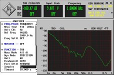
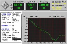
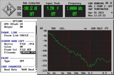
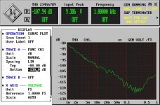
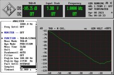
Here are the THD results, the Vcm value is in the screen shot names (left to right, the original 1.65V, then 1.2V, 1V, and 0.68V). Decreasing the Vcm from 1.65V apparently initially shifts the hump toward higher input values, then at 0.68V the hump is completely missing. Please note the Y change of scale on the 0.68V graph, the bottom is now -130dB. I have to double check, but I recall that the increase of THD towards FS is due to the insane levels (almost 20Vpp) that my R&D UPD starts to run into non linearities at.
I have to admit I have no clue why the changes in Vcm triggers such a dramatic change in the distortion profile, engineering based suggestions are welcomed.
P.S. I wonder if the same trick would help the ES9038Q2M.
Attachments
Last edited:
364mV.
This is for each half (4 channels in parallel). IV resistor is 49.9ohm. The DC value is exactly what I would expect, given the ES9038PRO output impedance of 202ohm (per channel).
P.S. The ESS9038PRO reference board uses Vcm=1V (with 8 individual channels). Much lower than AVCC/2, but higher than my 0.68V. Could be because I'm paralleling 8 channels? Unfortunately I don't have an ESS reference board, since those aholes refused to sell me one.
Last edited:
So how do the rest of the results stack up, with the change? no whack-a-mole? great job with the results and controlled testing and yes, for the memory recall of testing Mark. Pity to not know why though. I will replicate if I can, but I havent got a R&S or AP or functional equivalent around unfortunately, thats what i'm working towards. Any chance you would replicate testing on one of my 9038q2m boards syn08 if I send one to you syn08? i'll likely design in some test points to simplify for my own testing, SMA suit you? wouldnt be for a couple months, given postage times for PCBs and everything these days. not expecting you to troubleshoot for me, but setting for input common mode should be straight forward.
Last edited:
THD+N for Vcm=0.68V.
This is one good DAC chip . Confirmed, the raise of distortions toward full scale is a property of my R&S at the insane levels of 20Vpp. A 10dB attenuation in the 9038 registers removes the THD+N increase, but I am not sure how this volume control is working, I suspect it's on the digital side. So I'll build a 10dB analog attenuator (not a trivial task).
This is one good DAC chip
. Confirmed, the raise of distortions toward full scale is a property of my R&S at the insane levels of 20Vpp. A 10dB attenuation in the 9038 registers removes the THD+N increase, but I am not sure how this volume control is working, I suspect it's on the digital side. So I'll build a 10dB analog attenuator (not a trivial task).Attachments
The more I see of 9038 designs, the more I think Benchmark made a reasonable decision to use the 9028. At some point you're trading between optimizing for noise or distortion, and it's tough to use such a hot output. Analog attenuation always brings compromises as you mention.
Looking really good, though.
Looking really good, though.
Any chance you would replicate testing on one of my 9038q2m boards syn08 if I send one to you syn08?
Contact me when you are done. The hurdle will be cabling, as you see I am using SMA connectors all over, and for good reasons. I've learned the hard way that at these levels any improvised signal wiring (alligators, clips, etc...) come to a price, leading to much head banging against the bench.
Thanks mate, will do. Yes, I had already decided on building in test points. There is a part by HP that basically holds the probe, but I was thinking SMA would probably be better. Plus they (the HP part) are quite expensive for what they are. Problem (not really a problem) is, even those practically dwarf my board ... you can see in the pics how big just an SOIC8 is in comparison.
On that note, those rigid SMA connections look tough!. looks like a very serious instrument. Looking really good; I bet you are relieved. would you say you are all set to move on with your project now?
I dont mind the high output current, as i'll be using them in multichannel mode, so brings the output to a more manageable level.
On that note, those rigid SMA connections look tough!
. looks like a very serious instrument. Looking really good; I bet you are relieved. would you say you are all set to move on with your project now?I dont mind the high output current, as i'll be using them in multichannel mode, so brings the output to a more manageable level.
Last edited:
ASR Links:
ESS THD ‘Hump’ Investigation | Page 14 | Audio Science Review (ASR) Forum
...post #270
ESS THD ‘Hump’ Investigation | Page 14 | Audio Science Review (ASR) Forum ...post #280
ESS THD ‘Hump’ Investigation | Page 14 | Audio Science Review (ASR) Forum
...post #270
ESS THD ‘Hump’ Investigation | Page 14 | Audio Science Review (ASR) Forum ...post #280
.... So I'll build a 10dB analog attenuator (not a trivial task).
What are the challenges here if I may ask?
//
Thanks for that Mark. I hadnt read the whole thread, but had come across that schematic all by itself, without the accompanying calcs for proper setting of VGND inline with your IV stage and filter values. I saw it alone and it looked too much like a filter change (whack-a-mole) to me. So, hang on, this is as 'simple' as the virtual ground being set too high (at ~AVCC/2) as per their early application and, what, showing low level IMD riding on the signal, whatever the level of signal is at?? why wouldnt you tell people about that if you could solve it by reducing that level to below the onset and bam... free upgrade?
The calc was for an earlier chip. Also, seems to me it was still based on empirical results (experiments, he said in post 270), even if the results were presented formulaically. For a newer or different chip, newer experiments might be needed for optimization. Many people including me tend to stop studying the underlying cause of a problem once a fix is found. Deeper investigation would be nice to do, but it takes time that might be better spent finding a fix for some other remaining problem.
Last edited:
I have to double check, but I recall that the increase of THD towards FS is due to the insane levels (almost 20Vpp) that my R&D UPD starts to run into non linearities at.
Fond as I am of the illogical concept of running hot from the source into a low gain power amp that could make a very nice (if OTT from a performance perspective for music) front end.
Fond as I am of the illogical concept of running hot from the source into a low gain power amp that could make a very nice (if OTT from a performance perspective for music) front end.
Interesting enough, such a low gain power amplifier would be of a lower quality; reason is, at low closed loop gains, an amplifier is much more prone to be driven into instabilities, high closed loop gain amplifiers are much easier to be kept stable. Hence, a low closed loop gain amplifier has to be compensated more aggressively to maintain the stability margins at reasonable values.
Or the dual fact, if we assume the same unity loop gain frequency, a low closed loop gain amplifier needs to be unconditionally stable, there's no room for the phase to return to reasonable values after the dip in a dual pole compensation schema. This forces a low closed loop gain amplifier to be Miller compensated, which once again leading to lower loop gains, hence less distortion reduction.
The calc was for an earlier chip. Also, seems to me it was still based on empirical results (experiments, he said in post 270), even if the results were presented formulaically. For a newer or different chip, newer experiments might be needed for optimization. Many people including me tend to stop studying the underlying cause of a problem once a fix is found. Deeper investigation would be nice to do, but it takes time that might be better spent finding a fix for some other remaining problem.
Oh I realise it wont apply copy-paste to other chips and layouts, thus me doing this test build with the 9038q2m to practice technique with a lower cost in time and money in PCBs, before moving on to a 'final' multichannel build and to some degree repeating the method. I'm fairly certain i'm good to go with the layout concerns he mentions, so its a matter of experimental setting of the filter values/gain and then the hump, with those variables locked in place. Yes, it appears to be an applications engineer tackling the problem post-production, rather than operating with a known set of conditions and including that in the datasheet. So maybe awkward conversation to have with customers of an uber performance dac, admitting there is something they dont 100% understand going on with their parts.
Luckily its not a huge deal, as initially I plan to have the input board and MCU on a separate board anyway (not sure about master clock and reclock logic yet, but at first testing it will be on that board I think). I dont typically like these huge lego assemblies of different pcbs for everything though, so it will all go onto 2 or perhaps 3 boards for the whole music server/node, once its all working as designed.
Last edited:
And to conclude, this is probably the best of the best one could get out of a ES9038PRO chip in mono mode (8 channels in parallel).
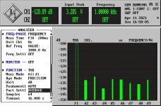
THD was optimized using the ES9038PRO compensation registers (0x1C - 0x1F). The impact on the 2nd harmonic cancellation is quite effective, around 8dB, which is somehow to be expected; probably the THD adjustment compensates for some internal asymmetries. The 3rd harmonic compensation adjustment has a minimum impact (less than 1dB). BTW, the datasheet description of register 0xC which, among others, controls the THD adjustment enable/disable is correct, correction is enabled by default (after a reset), bit6=0 means 'enabled' in this case.
Unfortunately, the THD compensation depends both on the input level and frequency. For this particular experiment I set the input level @0.35FS and frequency 1KHz. Going to 0.5FS and 2KHz increases again the 2nd harmonic to about -120dB (3rd harmonic remains largely unchanged at about -129dB). I'm also logically suspecting that this distortion minima is chip dependent. So this distortion minimum is largely of academic interest anyway (since it is far from the audible threshold anyways).
I guess I can pat myself for getting -128dB 3rd harmonic in my implementation, that's 10dB better than the Gustard X26 Pro using the same chip in the same mode. I'll do eventually a frequency and input level scan and plot THDto see how "bad" this can get over the entire audio band .
AKM and Rohm, beat this.
P.S. This is dedicated to the Jiteratti (© chris719) team; -129dB distortions with the Si570 clock @50MHz, having a jitter of 0.6pS RMS and an horrible close-in phase noise of (estimated) some -60dB @1Hz and some -90dB @10Hz.
THD was optimized using the ES9038PRO compensation registers (0x1C - 0x1F). The impact on the 2nd harmonic cancellation is quite effective, around 8dB, which is somehow to be expected; probably the THD adjustment compensates for some internal asymmetries. The 3rd harmonic compensation adjustment has a minimum impact (less than 1dB). BTW, the datasheet description of register 0xC which, among others, controls the THD adjustment enable/disable is correct, correction is enabled by default (after a reset), bit6=0 means 'enabled' in this case.
Unfortunately, the THD compensation depends both on the input level and frequency. For this particular experiment I set the input level @0.35FS and frequency 1KHz. Going to 0.5FS and 2KHz increases again the 2nd harmonic to about -120dB (3rd harmonic remains largely unchanged at about -129dB). I'm also logically suspecting that this distortion minima is chip dependent. So this distortion minimum is largely of academic interest anyway (since it is far from the audible threshold anyways).
I guess I can pat myself for getting -128dB 3rd harmonic in my implementation, that's 10dB better than the Gustard X26 Pro using the same chip in the same mode
. I'll do eventually a frequency and input level scan and plot THDto see how "bad" this can get over the entire audio band .AKM and Rohm, beat this
.P.S. This is dedicated to the Jiteratti (© chris719) team; -129dB distortions with the Si570 clock @50MHz, having a jitter of 0.6pS RMS and an horrible close-in phase noise of (estimated) some -60dB @1Hz and some -90dB @10Hz.
Attachments
Last edited:
THD was optimized using the ES9038PRO compensation registers (0x1C - 0x1F). The impact on the 2nd harmonic cancellation is quite effective, around 8dB, which is somehow to be expected; probably the THD adjustment compensates for some internal asymmetries. The 3rd harmonic compensation adjustment has a minimum impact (less than 1dB).
Maybe it so for 8 channels in parallel, but for 4 channels (2x4) I have seen much bigger impact on the 2nd and 3rd harmonics, and very low impact on 4th, 5th and higher.
Interesting enough, such a low gain power amplifier would be of a lower quality;
Hence my use of the work 'illogical'. But is does allow consideration of some interesting topologies that have been ignored (usually for very sensible reasons).
Anyway, sorry for the OT.
Maybe it so for 8 channels in parallel, but for 4 channels (2x4) I have seen much bigger impact on the 2nd and 3rd harmonics, and very low impact on 4th, 5th and higher.
Possible, I am suspecting the IV stage has also a large impact on the distortion cancellation, so an apple to apple comparison would be needed to decide.
I am using 2 x OPA1622 + OPA1611 for summation, can't imagine a better combination, low noise, low distortions, high current output for the OPA1622 with the low distortion of the OPA1611. IV resistors are 49.9ohm. The only shortcoming of this config is it denies the op amp rollers the opportunity to exercise their hobby, due to the weird, non standard, OPA1622 chip outline.
- Home
- Design & Build
- Equipment & Tools
- ADCs and DACs for audio instrumentation applications