Power dissipation is huge... Two channels running @100MHz, at 0dBFS eat up around 8W. On +5V (used for generating all 3.3V 1.2V using linear regulators) it takes about 1A (100mA is the Si570 oscillator, 80mA the digital buffers, the rest are the ES9038PRO plus it's regulators) while the I/V stages (4 double OPA1622 plus 4 OPA1611) take some 3W. Can be lowered using some switchers as pre-regulators, but I could hardly justify the complexity... After adding top and bottom cooling ground planes, this thing doesn't exceed 60-70 degrees centigrade temperature.
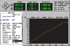
This is the SINAD. Peak is 113dB at about -6dBFS, from there it's the UPD which gives up at very high input levels (confirmed independently). Extrapolating the straight line gives a SINAD @0dBFS of about 122dB, which is IMO a great value. And no hump!
Attachments
Last edited:
I wish I could do that... Unfortunately my Rohde UPD has worse than -108dB THD residuals @20KHz, using the 100KHz analog analyzer.
Thanks for the info.
Some comments regarding the origins of the "hump" in the ES9038 products:
- It appears to affect most of the ESS DACs (certainly the ES9028 and 9038 series).
- For the ES9038 that I was able to measure, the outputs are firmly biased at AVCC/2=1.65V
- The output impedance is indeed around 200ohm per output.
- When the I/V stage common mode voltage is set lower than the AVCC/2 bias voltage, then a DC current flows through the I/V resistor to account for the bias difference. Example: AVCC/2=1.65V Vcm=1V R=50ohm results in a current of (1.65-1)/200~3.2mA. For 8 outputs in parallel, this amounts for about 25mA.
- This current comes from the opamp negative supply, since it is sunk by the I/V opamp. It increases the I/V stage standby power dissipation by a significant margin.
- The displaced Vcm bias is used by ESS in their demo boards (at least for the ES9038 series).
- Essentially, we are dealing with two voltage sources, Vcm and AVCC/2 fighting, and the resulting current flows through the DAC output impedance.
- No idea on how the ESS output stages are designed, but the fact that such a current flow practically eliminates the distortion hump suggests a mechanism similar with displacing the gm "hump" in older op amps with bipolar outputs, by biasing the output with a current source. This method eliminates the gm doubling distortion "hump" generated by the op amp output stage.
- If this is correct, the "hump" is essentially because of the poor output impedance of the ESS outputs (200 ohm parallel, or the Thevenin equivalent series impedance). A poor output impedance is also typical for op amps that can be improved by biasing the output.
I am afraid that's all we can speculate and infer about the "hump" origin, lacking any information from ESS.
ESS mentions you can use them both voltage out and current out. That always seemed to be a poor compromise but it would explain some of the odd behavior. Would a current source into the summing junction balance the output and correct the hump? It seems it would need to be really precise.
- If this is correct, the "hump" is essentially because of the poor output impedance of the ESS outputs (200 ohm parallel, or the Thevenin equivalent series impedance). A poor output impedance is also typical for op amps that can be improved by biasing the output.
Why did you call the output impedance "poor". Would you prefer to see a real Iout-DAC with (theoretically) infinite output impedance?
That would be nice, yes. Or at least a "true" current output, the ESS DACs in "current mode" are actually 200ohm impedance voltage output, feeding a virtual ground. These are quotes straight from the horses mouth (the ES9038PRO designer):
https://www.diyaudio.com/forums/dig...-reference-dac-8-channel-154.html#post2223575
https://www.diyaudio.com/forums/dig...-reference-dac-8-channel-140.html#post1814598
I'm suspecting the delta in performance between the "current mode" and the "voltage mode" is less because the ESS DAC and more because of the op amp common mode distortions. This would worth further investigations.
From what I understand the performance improvements also come from less voltage dependent resistor unlinearities inside the ESS chips when feeding a virtual ground.
I'm suspecting the delta in performance between the "current mode" and the "voltage mode" is less because the ESS DAC and more because of the op amp common mode distortions. This would worth further investigations.
Could be, but they tested with AD797 initially, and that has pretty decent performance as a follower.
From what I understand the performance improvements also come from less voltage dependent resistor unlinearities inside the ESS chips when feeding a virtual ground.
Interesting, how have you arrived at this conclusion?
I have not arrived at it, I'm merely repeating the explanation I heard from other people. It sounded reasonable though. And it goes something like this:
Resistors on silicon have a greater voltage-dependent nonlinearity than for example pretty linear metal film resistors. Keeping the output at a virtual ground level will make sure that the resistors always see the same voltage - either AVCC-Output or Output-GND.
If you use the DAC in voltage output mode the voltage across the resistors will be signal dependent (and possibly cause greater nonlinearites).
ESS DACs do not have a "current mode" and a "voltage mode" per se. The "mode" is actually defined by the input impedance of the following stage. If it's a virtual ground, it's in "current mode". If it is a high impedance, like a non inverting buffer, it's in "voltage mode".
The ES9038 chip designer mentioned that internally the chip can be modeled as an ideal voltage source, in series with a some 200ohm resistor. Since the input impedance of the buffer can be made extremely high (think of a jfet input op amp) in "voltage mode" there's virtually no current flowing through the resistor and any resistor voltage coefficient would be reduced to dust.
In "current mode", the equivalent model is an inverting op amp stage, where the 200ohm resistor is R1 and the I/V resistor is Rf, the gain is -Rf/R1=-Rf/200. Since R1=200ohm sees the entire voltage swing of the internal voltage source, logically a voltage coefficient would affect the current fed to the virtual node, and hence the inverting buffer output (practically R1=Rf since no real gain is required). So it is the "current mode" that would be more affected by the internal 200ohm impedance voltage coefficient.
So I don't think the explanation of the "voltage coefficient" holds water.
As of the origins of the output impedance fluctuations (likely responsible for the "hump"), I'd rather speculate that it's root cause is a "bug" in the 1 bit modulator selection (out of 1024 available) algorithm, or their grouping in slices of 4, per the ESS hyper stream patent. This technique (a new selection occurs at every conversion cycle) should theoretically convert distortions to noise, but apparently this process is not 100% efficient, otherwise the distortion correction registers would have no effect and would not be needed. It is IMO a distinct possibility that the 200ohm output impedance also fluctuates in each conversion cycle, but these fluctuations cannot be corrected from those registers.
I think I speculated enough for today 😀.
I don't think that a "black box" model of the DAC with just one resistor and one voltage source can be used to explain things here. There are actually N (N being a power of two, I think it's actually 32 forming a 5bit DAC, might be 64 though) resistors in there that are individually switched to AVCC or ground and are all connected at the output node. So each individual resistor will see varying voltages if the output voltage changes.
But I find it very interesting that somebody else is speculating about the hump, it's about time we started to do so here 🙂
I have to admit that I currently can't follow your theory but I will try harder, promise! Let me ask you one question though - if your theory is correct how can modifying the I/V stage make things worse/better. Does that go against or with your theory?
For the sake of completeness... Would you be willing to share the complete schematic to your DAC board? We're currently designing mono boards with the 9038Q2M and will have to solve the hump problem, too. So naturally I'm very interested in your explanations and measures against the hump!
EDIT: regarding the modification of the I/V stage: I mean modifying the R/C parallel to the I/V resistor.
Last edited:
I have no idea about if (and if so, how) modifying the I/V stage removes the hump in ES9038PRO. I know it was reported for the ES9038Q2M, but I have myself no experience with that. What I did is described in the last few pages: lowered the Vcm to 0.82V (coincidentally AVCC/4). Measurements before/after this change are shown.
You are describing exactly the mechanism of Rout fluctuations I mentioned in the previous post, and which has very little to nothing to do with a resistor voltage coefficient (which, BTW, could also not explain a "hump" but only an increasing distortions with the signal level, which was not observed). The model with a voltage source and it's internal impedance is what a user sees (without any insights, as a black box) and promoted by the chip designer.
As of sharing the schematic (I suppose you mean the I/V stages and the power supplies), it largely depends on who's "we are currently designing". Worst case, you will need to wait until the cake is thoroughly baked. However, for audio reproduction purposes, in my opinion the "hump" is only an academic and marketing issue. I understand that no DAC developer would like to see his baby measured by (for example) the guys @ASR, and have it "not recommended" because of a -100dB distortion hump.
Last edited:
OK, we are planning to have a pot to be able to adjust the value of the vref voltage for the i/v on the prototype board anyways, so we will watch out for that.
In the end this is still contrary to the findings of the developer of the sgd1 DAC which he made public in the asr forums:
How to Fix ESS Hump on SGD1 and LA-QXD1 | Audio Science Review (ASR) Forum
And yes, I'm especially interested in your I/v implementation. As to who "we" are - a friend of mine and me. No commercial stuff involved and everything will be open sourced after finishing. As is all my software already.
A pot is probably not the best idea, may I suggest using a low noise LDO like the LT3042 and a single 8.2K resistor to set the output voltage. Add 3pcs. of 10uF ceramic caps (input, output and decoupling), that's all it takes. Be prepared for the I/V op amps to dissipate some significant power, per my previous post.
I have not arrived at it, I'm merely repeating the explanation I heard from other people. It sounded reasonable though. And it goes something like this:
Resistors on silicon have a greater voltage-dependent nonlinearity than for example pretty linear metal film resistors. Keeping the output at a virtual ground level will make sure that the resistors always see the same voltage - either AVCC-Output or Output-GND.
If you use the DAC in voltage output mode the voltage across the resistors will be signal dependent (and possibly cause greater nonlinearites).
Others believe this is the mechanism but I think it is more likely the modulation of 'on' and 'off' resistance of the logic gates switching the resistor array due to OP swing.
It makes much more sense to me and you could probably simulate it.
I'm sure there are voltage related resistor distortions but they would surely be
much lower.
TCD
I found one article with info https://www.hindawi.com/journals/acmp/2015/423074/ it seems that at ic voltages volt coeffient is unlikely to be an issue.
Perhaps not an issue for high voltage applications (power devices?), where a <1% variation could likely be acceptable.
But since the curves of figure 2 show a variation over voltage that can easily be seen visually, I doubt that it will be possible to achieve a variation in the ppm or sub ppm region, which would be necessary to achieve very low distortion.
On-chip resistors can typically be made to match very well, but are typically not with well defined resistances. Or with low temperature and voltage dependence.
- Home
- Design & Build
- Equipment & Tools
- ADCs and DACs for audio instrumentation applications