Its possible to get pretty good metrics from a semi resistor : https://datasheets.maximintegrated.com/en/ds/MAX5492.pdf Its not clear what the process is here but it does have on chip ESD protection so it is some semi process.
Very poor resistors, likely diffused/implanted (since they have 30MHz bandwidth, meaning 0.5pF capacitance). Most DS specs refer to the resistor ratio, and even for that (e.g. Resistance-Ratio Accuracy vs. Voltage) are very bad. Also look at the THD+N, 0.002%, that is -94dB, a carbon film resistor value (and Johnson noise is 10k, 12.6nV/rtHz, 1.8uV in 20k BW, that is -115dB). Either the distortions are huge, or there is a lot of excess noise. Metal film resistors are under -140dB and have pretty much no excess noise to speak of. I would not use these resistors for audio, much less for instrumentation, other than for near DC voltage divider.
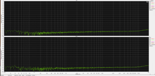
A screenshot from REW default settings from a 10 kHz Victor oscillator driving 50 ohms into a LTC2387-16 ADC board. The data was downsampled to 1.536 MHz with SoX. The gain structure and circuit is not optimized for this, and I don't think the oscillator is really enjoying the 50 ohm load.
Attachments
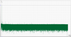
A screenshot from REW default settings from a 10 kHz Victor oscillator driving 50 ohms into a LTC2387-16 ADC board. The data was downsampled to 1.536 MHz with SoX. The gain structure and circuit is not optimized for this, and I don't think the oscillator is really enjoying the 50 ohm load.
Looks very good for 16bit, right on spot for the typical performance, makes me re-consider instead of the delta-sigma 24bit ADS127L01. The ADS has max 18 ENOB, a 20bit SAR may certainly exceed this. I'll take a second look... how did you convert from LVDS SPI to USB to PC? This must be more complex that the ADC setup itself, and quite high speed.
Looks very good for 16bit, right on spot for the typical performance, makes me re-consider instead of the delta-sigma 24bit ADS127L01. The ADS has max 18 ENOB, a 20bit SAR may certainly exceed this. I'll take a second look... how did you convert from LVDS SPI to USB to PC? This must be more complex that the ADC setup itself, and quite high speed.
Yeah, we also populated some boards with the 18-bit version but they are actually in use for real work. I think with an optimized implementation of that it could have near 20-bit performance at 48 kHz after filtering.
The interface isn't even SPI really, it's just DDR LVDS serialized data with a bit clock, but it's a real pain to interface with. You feed it a data/bit clock and it echoes it back to you on one of the LVDS pairs, but the clock and data are edge aligned. That means you have to delay one of them to capture the data, so an FPGA is probably mandatory. The rates sort of make it that way anyway. I forget the details from the timing diagrams already, but I had issues running the data clock at the minimum rate that would seem legal in one-lane mode. It ends up that 180 MHz worked for me for the 16-bit version (not 18 though), the evaluation board uses 360 MHz. There's also no frame signal. The data clock must be gated/gapped which means you can't create it directly with (or even bring it back into the FPGA) the Xilinx PLL IP (MMCM), because they don't have an option to maintain output when it stops. The situation is a bit easier with Intel/Altera parts.
After the data is deserialized it gets sent to the PC at the full 15 MSPS per channel through an FTDI FT600 FIFO to USB 3.0 chip. That is fairly straightforward, but does have some interesting errata and I spent a lot of time chasing down lost samples when it switches buffers internally. With the 16-bit FT600 you can push around 180-185 MB/s maximum for one IN endpoint. In theory you can do double that with FT601 but I suspect it doesn't scale perfectly. The board is also fully isolated from the USB host and FPGA using ADN465x LVDS isolators.
I think LTC2378-20 or LTC2380-24 might ultimately be better in the audio band if you don't need such a high sample rate. They will certainly be easier to interface with.
Last edited:
Yeah, I am trying instinctively to avoid FPGAs and CPLDs, I had a very basic introduction, did a few basic examples, and I was left with a terrible feeling of being on a hostile territory, with very limited weaponry to fight any significant battle. I may not have a choice and jump in sooner or later, or I may decide "I'm too old for this ****", don't know yet... It's a full time job to properly do these implementations, I don't see much room for amateurs like myself, in particular since the IPs are not free, so one is supposed to re-invent the wheel, certainly in rudimentary ways.
And some good news...
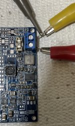
Since I had anyway some other PCBs in the work @JLCPCB, I spent another 5 bucks and ordered a revised board for the pesky LT8582 feedback controlled switcher. Some major changes compared with the original schematic in the LT3094 data sheet (and the AN mentioned by somebody here). The positive supply now has the slow start PMOS added, while the negative supply was outfitted with the coupled dual inductor. Everything re-calculated using a spreadsheet that automates the outlines in the LT8582 data sheet, works like a charm. So essentially I was right, the simplest positive supply blows at startup for low input voltages (5V in my case), meaning high current through the switches, if there is no slow start up schema. I have tested for all input voltages between 4V and 13V (for output voltages from the linear regulators of +/-15V and it works perfectly, no output noise to speak of, etc... Switching is at 1.5MHz.
New schematic and a photo of the relevant board area are attached.
And some good news...
BTW, don't ask me how I learned, but the interesting schematic https://www.analog.com/media/en/technical-documentation/data-sheets/LT3094.pdf page 30 is on the bench a silicon graveyard. Both the LT8582 and the LT3045 are destroyed at the first power up, I've burned $100 in chips while experimenting. Still don't know exactly why it does this, but I assume is the missing P-Channel MOSFET on the positive rail. Per the LT8582 datasheet, this MOSFET allows the positive rail soft start, without this the LT8482 blows (since the control voltage from the LT3045 doesn't have a chance to settle and the converter is in full throttle until it would), and the spikes take out the LT3045 as well.
Since I had anyway some other PCBs in the work @JLCPCB, I spent another 5 bucks and ordered a revised board for the pesky LT8582 feedback controlled switcher. Some major changes compared with the original schematic in the LT3094 data sheet (and the AN mentioned by somebody here). The positive supply now has the slow start PMOS added, while the negative supply was outfitted with the coupled dual inductor. Everything re-calculated using a spreadsheet that automates the outlines in the LT8582 data sheet, works like a charm. So essentially I was right, the simplest positive supply blows at startup for low input voltages (5V in my case), meaning high current through the switches, if there is no slow start up schema. I have tested for all input voltages between 4V and 13V (for output voltages from the linear regulators of +/-15V and it works perfectly, no output noise to speak of, etc... Switching is at 1.5MHz.
New schematic and a photo of the relevant board area are attached.
Attachments
Last edited:
Yeah, the FPGAs and tools are not very friendly. Most of the IP you would need is free on the Xilinx side, but it is a very frustrating experience overall. Vivado LOOKS nice but it's a seriously buggy mess if you use the GUI workflow and Intel Quartus is not much different. I don't do a lot of HDL for my day job, but I know that the guys that do truly complex work have to ignore the GUI and only use Python and TCL commands to drive everything. It takes a lot of setup and learning.
If you do jump in, I would recommend VHDL over Verilog. Less likely to shoot yourself in the foot because of software habits.
Good to know on the switcher. I can't remember what I used on the ADC board but it was a separate boost and inverting (Cuk) boost. No fancy VIOC because the power budget or voltage drop wasn't an issue.
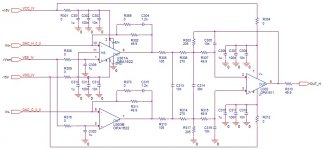
I/V stages are frozen, so here's the schematic I am currently using. It's a classic filter design (AC wise) so I will not comment on that.
Some comments:
- Full scale output is about 4Veff (for an ES9038PRO configured in mono mode)
- All signal path capacitors are C0G
- All decoupling caps are X7R
- No electrolytics or tantalums are used; the +/-15V supply has 22u X7R at the LT3045/LT3094 outputs.
- Make sure you provide some PCB cooling for U301 by soldering the tab to a copper area (connected to -15V); U301 runs pretty hot, as described in another post.
- This is half of the I/V needed for balanced output, a total of 4 channels are used for a dual mono ES9038PRO.
- You can omit the 0 (zero) ohm resistors, they are only placeholders, in case any extra local extra RC decoupling would be required. At least in my PCB layout (four layers) they were not required.
- R369/R370 are placeholders for implementing the "anti-hump" topology; after finding that Vcm adjusting to 1/4AVcc eliminates the hump, they are no longer required.
- All resistors in the signal path are 0.1% thin film. I used 0603 all over, no problems detected due to power dissipation. Those inclined to be more conservative may use 1206 0.1% for the I/V resistors (49.9ohm)
Attachments
Last edited:
What is the peak current through through the 49.9 Ohm resistor? That's what I would use to scale its size.
That's enough current to justify a bigger resistor. Not for power but for stability and etc. If you were really clever you could match it to the internal resistance TCR & HF nonlinearity but I think madness would lie down that path in this case.
ES9822 still impressing me, it already outperforms my AP SYS2*** regarding THD+N, even in stereo-mode -119db, and mono -121db.
AP SYS2522 + external LPF to final clean up is my 1kHz test signal. BW is standard 20-22000Hz. No idea why ESS specified just -117/118db, maybe also SYS2*** limitation, probably their LDO not as good as my opamp instead of ES9311.
Last edited:
Thanks. Could perhaps some noise shaping be involved, resulting in correspondingly increased noise in higher frequencies (outside of the audio band, but still well within instrumentation/measurement band)?
Per ESS they pushed the noise shaping up to 200K as a start point. They also mention using an external FPGA to do "things". I still find their attitude pretty obnoxious and arrogant. And getting parts from them can be quite difficult if you are not a major player.
I tend to say that it is flat up to 80-100k at Fs = 384k. I don't wanna use that chip > 384k yet for economical reasons(CT7601SR bridge) and due to USB port 5V rail current limit(500mA already). Yesterday I did calibrate my 9038D DAC+HPA with that Cosmos ADC and got nearly perfect matching with AP SYS2522 result i.e. -130-135db harmonics level is reliably available with the ADC 90x50mm PCB. As I already said, THD+N performance of that ADC better than SYS2522 THD+N analog analyzer for 1-1.5db(AP -119.5db vs Cosmos -121db). When I'll get the sample of housing for the ADC, I'll take a picture to compare the size of AP SYS2522 vs Cosmos ))
Attachments
Last edited:
Per ESS they pushed the noise shaping up to 200K as a start point. They also mention using an external FPGA to do "things". I still find their attitude pretty obnoxious and arrogant. And getting parts from them can be quite difficult if you are not a major player.
What "things"? Seems strange unless they are doing what TI did with PCM4222 and allowing you access to the modulator output so you could implement better filters externally.
- Home
- Design & Build
- Equipment & Tools
- ADCs and DACs for audio instrumentation applications