We could use a FPGA or ASIC, however, the nasty thing here is that we need to reduce (switching) noise to lowest practical level and that's going to be extremely difficult with these LSI chips that produce very strong interference. Even a tiny PAL (Programmable Array Logic) produces massive switching noise and draws a lot of current...
I would like to know if you have a reference for this with newer devices. The MachX02 FPGA I am using (which is barely more than a CPLD) consumes only a little over 1.5mA static current in operation. Dynamic current and noise should be lower than a sea of discrete devices due to the fact that each 74xxx device used in a discrete implementation has its own output driver. These output drivers are large, hungry, and noisy compared to the small process internal devices within the FPGA. Only the 4 output pins of the FPGA have larger drivers attached and their drive current capability can be programmed.
Perhaps in the past FPGAs were hungry and noisy, but I'd like to know if that is still the case with new devices on small, power-efficient processes. From my own research and the math involved, these new small devices seem like a much preferred option to individual discrete devices for lower noise (when properly bypassed according to the manufacturer recommendations) and power consumption.
raptorlightning said:Perhaps in the past FPGAs were hungry and noisy, but I'd like to know if that is still the case with new devices
I don't think you will get the ultimative answer to this question. You should try and see if it will work.
If you want I can send you my discret logic board as a reference. Or you can buy discrete I2S2PCM board from ryanj.
I agree with raptorlightning. Old CPLDs also used to be resister loaded dynamic logic to make "wired AND" stage thus they were more noisy and may prone to jitter. It is not today's story.
But subjective preferences can't be eliminated from our audio world. We don't need to cling such old DAC chips from objective perspective...Then logic ICs.
But subjective preferences can't be eliminated from our audio world. We don't need to cling such old DAC chips from objective perspective...Then logic ICs.
Hi weissi,
TDA1541A performs best by far when driving it in signed magnitude mode because:
Low level distortion and switching noise will be reduced significantly as only few bits change around the zero crossing and the monotonicity of the DAC improves.
If one is concerned about channel matching (this causes ever so slight even order harmonics distortion that is not objectionable) following can be done:
Put 100K ... 1M multi turn trimmers in parallel with each 150R passive I/V resistor and sum both outputs with say 1K resistors. Then trim for best channel / segment matching.
I am not quite sure what you are saying here?
Is it between L and R channel or is it the channel difference between the two DAC's inside one TDA1541A that is used to form the single Signed Magnitude
DAC?
If your are talking about the last situation, then I do not think this could work , as you have to connect the two 150 Ohm resistors when done, and then nothing has been gained. If you use one 150 ohm on each of the DAC's (DAC- and DAC+) and sample the two outputs with 1 KOhm resistors, you get severe distortion at least with full scale digital input.
But you are right, higher even order distortion can be seen @ the output in Signed Magnitude operation with the two DAC's connected together and 75 Ohms to gnd.
Hi Hans Polak,
The MOS16 and MOS24 are based on single ternary logic (3 level logic) converters with impedance scaling for low output impedance, high accuracy and very low bit switching noise levels . Each ternary bit is controlled by two binary bits.
Both binary bits that form one ternary bit are powered by the same 4V battery power supply:
0 0 -> 0V reference 2V -> -2V output
1 0 -> 2V reference 2V -> 0V output
0 1 -> 2V reference 2V -> 0V output
1 1 -> 4V reference 2V -> +2V output
I use a +2V (exactly halve the battery power supply, tracking) as GND reference for the RCA outputs for DC-coupled output. The ternary converter offers 750 Ohm output impedance and 4Vpp output.
So I do not use two R2R ladder DACs in signed magnitude and have their outputs connected. I just use one single ternary logic converter for each channel.
This is how the output signal could be formed by the two groups of binary bits that form a group of ternary bits:
GRP1 GRP2
000 000 -7
001 000 -6
010 000 -5
011 000 -4
100 000 -3
101 000 -2
110 000 -1 <-
111 000 0 <-
111 001 +1 <-
111 010 +2
111 011 +3
111 100 +4
111 101 +5
111 110 +6
111 111 +7
GRP1 represents the lower binary bits group that control each ternary bit, GRP2 represents the higher binary bits group that control each ternary bit.
This logic is mirror symmetric:
GRP1 GRP2
000 000 -7
000 001 -6
000 010 -5
000 011 -4
000 100 -3
000 101 -2
000 110 -1
000 111 0
001 111 +1
010 111 +2
011 111 +3
100 111 +4
101 111 +5
110 111 +6
111 111 +7
So the groups have no particular polarity, it's just two groups of binary bits that form one group of ternary bits. When we swap the data into the segments of a signed magnitude DAC, output polarity will change as one DAC performs the positive signal halve and the other the negative signal halve.
Similar to a signed magnitude converter we can see that a ternary logic converter steps away from the zero crossing with small steps. Since both binary drive sections share the same supply, there is no need to use balanced power supplies like with signed magnitude converters.
The resistor matrix between the binary circuits that form the ternary circuit also provide D/A conversion by means of binary weighted ternary bits.
I have experimented with tri-state "disconnected" logic that electrically disconnects the D/A converter from the decoder after loading the data. But after switching to battery power supply this tri-state logic offers no advantages.
Yes I did, DI-8 vs 8 x TDA1541A in parallel. The overal sound quality of the DI-8 DAC was better (more natural, involving, and anlogue with stunning midrange). The trebles roll-off however is clearly audible and requires compensation. I experimented with analogue resonant treble booster filters and short FIR filters for boosting trebles.
What I understood from your latest version made with a DAC of your own, is that you are using dac's in sign magnitude set up, driving tri state buffers, from a + and - supply, making that the output has no DC offset, very clever.
The MOS16 and MOS24 are based on single ternary logic (3 level logic) converters with impedance scaling for low output impedance, high accuracy and very low bit switching noise levels . Each ternary bit is controlled by two binary bits.
Both binary bits that form one ternary bit are powered by the same 4V battery power supply:
0 0 -> 0V reference 2V -> -2V output
1 0 -> 2V reference 2V -> 0V output
0 1 -> 2V reference 2V -> 0V output
1 1 -> 4V reference 2V -> +2V output
I use a +2V (exactly halve the battery power supply, tracking) as GND reference for the RCA outputs for DC-coupled output. The ternary converter offers 750 Ohm output impedance and 4Vpp output.
So I do not use two R2R ladder DACs in signed magnitude and have their outputs connected. I just use one single ternary logic converter for each channel.
This is how the output signal could be formed by the two groups of binary bits that form a group of ternary bits:
GRP1 GRP2
000 000 -7
001 000 -6
010 000 -5
011 000 -4
100 000 -3
101 000 -2
110 000 -1 <-
111 000 0 <-
111 001 +1 <-
111 010 +2
111 011 +3
111 100 +4
111 101 +5
111 110 +6
111 111 +7
GRP1 represents the lower binary bits group that control each ternary bit, GRP2 represents the higher binary bits group that control each ternary bit.
This logic is mirror symmetric:
GRP1 GRP2
000 000 -7
000 001 -6
000 010 -5
000 011 -4
000 100 -3
000 101 -2
000 110 -1
000 111 0
001 111 +1
010 111 +2
011 111 +3
100 111 +4
101 111 +5
110 111 +6
111 111 +7
So the groups have no particular polarity, it's just two groups of binary bits that form one group of ternary bits. When we swap the data into the segments of a signed magnitude DAC, output polarity will change as one DAC performs the positive signal halve and the other the negative signal halve.
Similar to a signed magnitude converter we can see that a ternary logic converter steps away from the zero crossing with small steps. Since both binary drive sections share the same supply, there is no need to use balanced power supplies like with signed magnitude converters.
The resistor matrix between the binary circuits that form the ternary circuit also provide D/A conversion by means of binary weighted ternary bits.
I have experimented with tri-state "disconnected" logic that electrically disconnects the D/A converter from the decoder after loading the data. But after switching to battery power supply this tri-state logic offers no advantages.
After this long introduction, a simple question: in this sim the advantage of time shifting didn't become obvious, so I'm just curious whether you have auditioned this setup to a version where no time shifting takes place with just 4 Dac's parallel in time.
Yes I did, DI-8 vs 8 x TDA1541A in parallel. The overal sound quality of the DI-8 DAC was better (more natural, involving, and anlogue with stunning midrange). The trebles roll-off however is clearly audible and requires compensation. I experimented with analogue resonant treble booster filters and short FIR filters for boosting trebles.
Hi xaled,
Perhaps it's best to wait with a new design.
There might be an issue with 1 sample delay between L and R channel, koldby could check this out as I no longer have the test setup (recycled). Feed a 1 KHz stereo test signal into the DAC and observe both output signals. These should be perfectly aligned. If not, the window has to move to the WS=1 zone by replacing U3 with a 74LVC80 (inverted output). This requires no PCB change.
The decoding circuit can be simplified using one 74XX139 and 5 inverters (74xx04). It replaces U14 (74xx08), U15 and U16. This modification fixes the data muting problem on DOL- and DOR- and also offers all required data signals for a balanced segmented TDA1541A project.
Now that kolby got the board running I will update the current version of the board to include fixes for identified issues.
There is the open question for the need of AND gates at the output, to avoid the unwanted data in DOL- and DOR-. I will include the gates if there will be no comments against them or a proposal for a better solution.
Including the gates and other improvements will require some rerouting on the board and this will take some time.
I also want to get the I2S to Sign board to be useful in a stackable mode to have a dual TDA1541 board stackable on top of it. I will also try to design the right TDA1541 single ended board. Any cooperation on this would be appreciated.
I'm only interested in SE mode, but I know that there is also interest in balanced mode.
Is there any advantage for balanced mode with signed magnitude TDA1541 and I/V transformers that provide balanced mode on the secondary side?
Perhaps it's best to wait with a new design.
There might be an issue with 1 sample delay between L and R channel, koldby could check this out as I no longer have the test setup (recycled). Feed a 1 KHz stereo test signal into the DAC and observe both output signals. These should be perfectly aligned. If not, the window has to move to the WS=1 zone by replacing U3 with a 74LVC80 (inverted output). This requires no PCB change.
The decoding circuit can be simplified using one 74XX139 and 5 inverters (74xx04). It replaces U14 (74xx08), U15 and U16. This modification fixes the data muting problem on DOL- and DOR- and also offers all required data signals for a balanced segmented TDA1541A project.
Could somebody point out a successful design based on only one tda1541 chip for both channels? I mean a real schematic that delivers a good sound.
Search for red baron board, then search for 50Hz dem mod on this thread. This would be the best current practice.Could somebody point out a successful design based on only one tda1541 chip for both channels? I mean a real schematic that delivers a good sound.
The decoding circuit can be simplified using one 74XX139 and 5 inverters (74xx04). It replaces U14 (74xx08), U15 and U16. This modification fixes the data muting problem on DOL- and DOR- and also offers all required data signals for a balanced segmented TDA1541A project.
Thank you!
Hi, I´m catching up with the latest developments here... 🙂
Koldby, I believe John means a summing amp with 1K input resistors.
If someone wanted to try this (trim the upper and lower halves and thus lower THD) then it could be done discretly: a current to voltage converter with the aforementioned 1K resistors before the low impedance (summing) node.
(BTW, I did not implement the sign magnitude yet... it´s on the project list though)
-Alex
I am not quite sure what you are saying here?
Is it between L and R channel or is it the channel difference between the two DAC's inside one TDA1541A that is used to form the single Signed Magnitude
DAC?
If your are talking about the last situation, then I do not think this could work , as you have to connect the two 150 Ohm resistors when done, and then nothing has been gained. If you use one 150 ohm on each of the DAC's (DAC- and DAC+) and sample the two outputs with 1 KOhm resistors, you get severe distortion at least with full scale digital input.
But you are right, higher even order distortion can be seen @ the output in Signed Magnitude operation with the two DAC's connected together and 75 Ohms to gnd.
Hi xaled,
I made a new schematic for the I2S to (balanced) segmented decoder.
Decoding is simplified using the 74LVC139 decoder / demultiplexer.
Inverted and non-inverted signals are available for SE (2 x TDA1541A) and balanced (4 x TDA1541A) DACs.
Data muting is fixed by using the /E inputs of the 74LVC139. "0" on this /E input will enable the outputs. When outputs are disabled, all outputs are "1". because the 74LVC139 is enabled with a "0" U3 is changed to an OR gate (74LVC1G32).
BCKO has to be enabled with a "1" so an inverter (U2) is added
The remaining 6 inverters (purple) are part of a 74LVC04 HEX inverter.
The window has been moved to WS=1 zone by using a 74LVC80 (U7) to reset the counter and enable the window. Left data is loaded first while WS=0 and put through the 32 bit delay line. When WS=1 the R channel data is clocked out together with the delayed and now aligned L channel data.
U5 ... U10 may be replaced by 3 x 74LVC74. Verify that the correct outputs are used, 74LVC79 -> use Q output of the 74LVC1G74, 74LVC1G80 (use /Q output of the 74LVC1G74).
The outputs for a SE version are indicated with an asterisk (*).
Attachments

Hi koldby,
There are tolerances between L and R channel full scale current and tolerances between full scale current of different TDA1541A chips.
The full scale current equals approx. -4mA.
Put a separate 150R I/V resistor & +2mA bias current on each of the segment outputs. Now sum both outputs together using a summing circuit (2 x 1K resistor to a summing node for example). It is important that the 1K resistors come -after- the I/V resistor, not between TDA1541A output and I/V resistor!
Now you can trim one 150R I/V resistor, so that the full scale currents for both segments are exactly the same. By varying the I/V resistor value slightly, the ac voltage across that I/V resistor and related full scale voltage will also vary slightly.
One could also use a step-up transformer with multiple primary windings for summing the segment outputs.
I am not quite sure what you are saying here?
Is it between L and R channel or is it the channel difference between the two DAC's inside one TDA1541A that is used to form the single Signed Magnitude
DAC?
There are tolerances between L and R channel full scale current and tolerances between full scale current of different TDA1541A chips.
The full scale current equals approx. -4mA.
If your are talking about the last situation, then I do not think this could work , as you have to connect the two 150 Ohm resistors when done, and then nothing has been gained. If you use one 150 ohm on each of the DAC's (DAC- and DAC+) and sample the two outputs with 1 KOhm resistors, you get severe distortion at least with full scale digital input.
Put a separate 150R I/V resistor & +2mA bias current on each of the segment outputs. Now sum both outputs together using a summing circuit (2 x 1K resistor to a summing node for example). It is important that the 1K resistors come -after- the I/V resistor, not between TDA1541A output and I/V resistor!
Now you can trim one 150R I/V resistor, so that the full scale currents for both segments are exactly the same. By varying the I/V resistor value slightly, the ac voltage across that I/V resistor and related full scale voltage will also vary slightly.
One could also use a step-up transformer with multiple primary windings for summing the segment outputs.
But that was exactly what I did and got severe distortion @ full scale. Maybe I should try it again...Hi koldby,
There are tolerances between L and R channel full scale current and tolerances between full scale current of different TDA1541A chips.
The full scale current equals approx. -4mA.
Put a separate 150R I/V resistor & +2mA bias current on each of the segment outputs. Now sum both outputs together using a summing circuit (2 x 1K resistor to a summing node for example). It is important that the 1K resistors come -after- the I/V resistor, not between TDA1541A output and I/V resistor!
Now you can trim one 150R I/V resistor, so that the full scale currents for both segments are exactly the same. By varying the I/V resistor value slightly, the ac voltage across that I/V resistor and related full scale voltage will also vary slightly.
One could also use a step-up transformer with multiple primary windings for summing the segment outputs.
I still do not think this works properly.Hi koldby,
Put a separate 150R I/V resistor & +2mA bias current on each of the segment outputs. Now sum both outputs together using a summing circuit (2 x 1K resistor to a summing node for example). It is important that the 1K resistors come -after- the I/V resistor, not between TDA1541A output and I/V resistor!
Now you can trim one 150R I/V resistor, so that the full scale currents for both segments are exactly the same. By varying the I/V resistor value slightly, the ac voltage across that I/V resistor and related full scale voltage will also vary slightly.
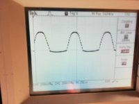
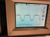
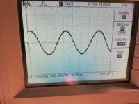
Pic.27 shows the summed output from the two 1KOhm resistors connected to each of the 150 Ohm resistorsthat is connected between the outputs of TDA1541A and ground.
Pic 28 & 29 shows the signal on each of the outputs directly across the 150 Ohms and with the two 1 KOhm in series connecting the two 150 Ohm.
Pic 29 shows the outputs when connecting the two 150 Ohms (and thereby also the two outputs)(short circuit the two 1KOhm resistors).
Now I speculate, and I have been known to be error prone in this art at times 🙂o), that this comes from the special behavior of the DO- outputs. When you look at the outputs only with 150 Ohm to ground and not connected together, the DO+ is a perfect half sinus going positive and ,with proper bias resistor, with a baseline @ 0V.
But if you look at the DO-, you have a perfect half sinus going negative and a baseline @ 0 V without a bias resistor. I think it is because the DAC that handles the DO- is loaded with 1111111111111111 with no digital input to the Signed Magnitude converter and therefore puts out 0 mA into the 150 Ohm resistor.
I am not sure why the outputs are behaving as they do, with a 2KOhm resistor( the two 1KOhm resistors in series) connected between them.
Attachments
Hi xaled,
I made a new schematic for the I2S to (balanced) segmented decoder.
Hi ecdesigns,
I'm reworking my board to interface stacked TDA board(s) and this will be the basis for it.
As always I highly appreciate your input.
After working more with the signed magnitude converter , I have realized, that the bias and I/V component values are actually wrong.
It is because the two dac's (dac+ and dac- ) are not working in parallel.
The dac+ is the only one that needs 2 mA bias and therefor the bias resistor must be 2.5 kOnms and it can only swing to + 2mA and the dac- do not need bias (all its current sources is off when not getting any data) and wil only swing to -2mA as it does not receive data that will make it swing further negative.
So the combination of the two dac's can only swing +/- 2mA and not +/- 4 mA and therefore the I/V resistor should be 150 Ohm and not 75 Ohm to make the same voltage swing as a TDA1541A working normally.
Hmm.
75 Ohms it must be as it clips like crazy with 150 Ohms and full scale input. I am not sure I understand why .
75 Ohms it must be as it clips like crazy with 150 Ohms and full scale input. I am not sure I understand why .
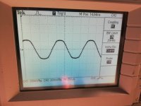
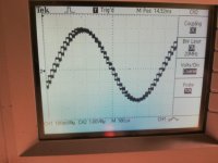
Hi Kolby,Here is a picture of the phase difference between L and R, as John mentioned.
How do you plan to compensate this phase difference?
- Home
- Source & Line
- Digital Line Level
- Building the ultimate NOS DAC using TDA1541A