IF we insist using a noisy ASIC or CPU we have to ensure that the D/A converter is -completely- shielded (EMI included) from this switching noise, I wish you good luck with that.
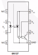
I don´t expect to better one of your excellent solutions John, but I believe this is a tool that might help me: 6N137
(This is for bitclock and data only. Not for wordclock.)
0.6pF capacitance between the LED terminals and the output side.
Quoting the datasheet: "An internal noise shield provides superior common
mode rejection of typically 10kV/µs."
The open collector makes it easy to implement the "reduced swing" for lowest tda1541 on-chip bounce.
Thanks,
Alex
Attachments
Hi John
I'm really happy you're looking at the TDA again! I've been reading this thread for a long time and although the mosaic was brilliant, I think there's a lot of us here in DIY land that appreciate your somewhat sideways approach to TDA perfection. 😉
An idea I've had for a long time but not got round to, is to try clocking the TDA with a SINE wave clock for BCK. As long as the voltage of the wave is high enough in combination with the frequency - in order to keep the slew rate high enough for reliable triggering of the TDA - then there should be great benefits to the noise amount/spectrum inside the TDA.
I'm not in a position to try it at the moment, but we have two options;
1) NOS - requires custom XTAL at 2.8...MHz but probably best solution at the end
2) 4 x OS - uses 11.286...MHz XTAL but possible degradation due to OS. I was thinking this is relatively interesting as a proof of concept ?
Thanks for the years of contributions
James
P.S. if you don't regularly read John Broskies Tubecad blog then check out the Digital Electrostatic speaker article - very off the wall and an interesting concept
I2S Input
Hello John,
Just did a quick draft in eagle based on your description for I2S input. I'm not that experienced in digital logic so could you please comment if the changes are correct?
>hat we have to do now is adding one extra D flip-flops to sample the MSBs one and a half bit after a WS change (1.5 bit delay) and a
The most uncertain part - did I get it right with the additional flip-flop?
>2 bit delay to drive the window generator so we still loose the MSB.
Connect U6 Q5 Pin to U17.
>DOL becomes DOR and DOR becomes DOL (swap channels) and we are ready to use I2S input signal.
Change output labels.
Could you also comment on the decoupling caps for digital logic? What values for capacitors, should all of the ICs be decoupled?
Thanks,
xaled
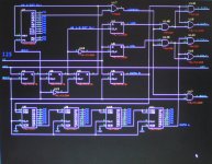
I2S to Signed Magnitude converter for 2 x TDA1541A
Hi xaled,
I assume your aim is to construct a I2S to signed magnitude converter.
You connected the Q output of the flip-flop Q3 to the output of NAND gate U17. This won't work as planned.
MSB sample flip flops U4a and U4B sample WS on 1BCK delay when MSB data is not valid for I2S.
I attached a schematic for I2S to signed magnitude converter for 2 x TDA1541A.
With I2S we have the left channel data available 1 bit after after WS goes low and the right channel data available one bit after when WS goes high.
With Left Justified we have left channel data available immediately after WS goes high and Right channel data available immediately after WS has gone low (schematic from my previous post).
In order to sample MSBs we need a 1.5 bit delay. Now we sample MSB half a BCK period after it has changed. This is provided by cascading flip flops . First one gives 0.5 bit delay and the second one flips over one BCK clock period later on 1.5 bit delay.
MSB for Right channel is available after WS has gone high (U4) and MSB for Left channel is available after WS has gone low (U5, inverted WS).
The Window signal needs to be shifted exactly 2 bits. We have 0.5 bit delay after U1, 1.5 bit delay after U2 and exactly 2 bit delay after U3. This 2 bit delayed WS signal is used to start the window counter by releasing its reset input. After 16 BCK pulses the output Q5 goes high. When we XNOR this signal with the 2 bit delayed WS signal we get the desired 16 bit window at the correct position.
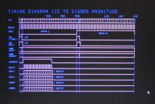
I also added a timing diagram for this slightly modified converter.
I haven't tested this schematic yet, it's based on theory. The Left Justified version has been tested in practice.
Use 0.1uF ceramic 805 decoupling caps. Look at my prototype board of the protocol converter for amount and location of the decoupling caps.
I would suggest to use 2V4 supply voltage for this decoder in order to minimise switching noise. Decoupling is not that critical here as the circuit draws very little current. I would place decoupling caps close to every counter, shift register and flip-flop and add a few more for all the gates.
Hi xaled,
I assume your aim is to construct a I2S to signed magnitude converter.
You connected the Q output of the flip-flop Q3 to the output of NAND gate U17. This won't work as planned.
MSB sample flip flops U4a and U4B sample WS on 1BCK delay when MSB data is not valid for I2S.
I attached a schematic for I2S to signed magnitude converter for 2 x TDA1541A.
With I2S we have the left channel data available 1 bit after after WS goes low and the right channel data available one bit after when WS goes high.
With Left Justified we have left channel data available immediately after WS goes high and Right channel data available immediately after WS has gone low (schematic from my previous post).
In order to sample MSBs we need a 1.5 bit delay. Now we sample MSB half a BCK period after it has changed. This is provided by cascading flip flops . First one gives 0.5 bit delay and the second one flips over one BCK clock period later on 1.5 bit delay.
MSB for Right channel is available after WS has gone high (U4) and MSB for Left channel is available after WS has gone low (U5, inverted WS).
The Window signal needs to be shifted exactly 2 bits. We have 0.5 bit delay after U1, 1.5 bit delay after U2 and exactly 2 bit delay after U3. This 2 bit delayed WS signal is used to start the window counter by releasing its reset input. After 16 BCK pulses the output Q5 goes high. When we XNOR this signal with the 2 bit delayed WS signal we get the desired 16 bit window at the correct position.
I also added a timing diagram for this slightly modified converter.
I haven't tested this schematic yet, it's based on theory. The Left Justified version has been tested in practice.
Use 0.1uF ceramic 805 decoupling caps. Look at my prototype board of the protocol converter for amount and location of the decoupling caps.
I would suggest to use 2V4 supply voltage for this decoder in order to minimise switching noise. Decoupling is not that critical here as the circuit draws very little current. I would place decoupling caps close to every counter, shift register and flip-flop and add a few more for all the gates.
Attachments
Sorry guys, totally OT. 😱
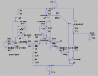
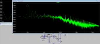
My low thermal memory mod for the diffamp, excellent sounding for balanced output DACs.
When both branches of the compound-Sziklai share equal currents, lower noise floor can be achieved.
Edit: added FFT for +/-24V supplies and 3.1mA passive CCS.
Cheers,
M.
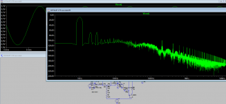
My low thermal memory mod for the diffamp, excellent sounding for balanced output DACs.
When both branches of the compound-Sziklai share equal currents, lower noise floor can be achieved.
Edit: added FFT for +/-24V supplies and 3.1mA passive CCS.
Cheers,
M.
Attachments
Last edited:
Hi John,Hi xaled,
I assume your aim is to construct a I2S to signed magnitude converter.
You connected the Q output of the flip-flop Q3 to the output of NAND gate U17. This won't work as planned.
MSB sample flip flops U4a and U4B sample WS on 1BCK delay when MSB data is not valid for I2S.
I attached a schematic for I2S to signed magnitude converter for 2 x TDA1541A.
With I2S we have the left channel data available 1 bit after after WS goes low and the right channel data available one bit after when WS goes high.
With Left Justified we have left channel data available immediately after WS goes high and Right channel data available immediately after WS has gone low (schematic from my previous post).
In order to sample MSBs we need a 1.5 bit delay. Now we sample MSB half a BCK period after it has changed. This is provided by cascading flip flops . First one gives 0.5 bit delay and the second one flips over one BCK clock period later on 1.5 bit delay.
MSB for Right channel is available after WS has gone high (U4) and MSB for Left channel is available after WS has gone low (U5, inverted WS).
The Window signal needs to be shifted exactly 2 bits. We have 0.5 bit delay after U1, 1.5 bit delay after U2 and exactly 2 bit delay after U3. This 2 bit delayed WS signal is used to start the window counter by releasing its reset input. After 16 BCK pulses the output Q5 goes high. When we XNOR this signal with the 2 bit delayed WS signal we get the desired 16 bit window at the correct position.
I also added a timing diagram for this slightly modified converter.
I haven't tested this schematic yet, it's based on theory. The Left Justified version has been tested in practice.
Use 0.1uF ceramic 805 decoupling caps. Look at my prototype board of the protocol converter for amount and location of the decoupling caps.
I would suggest to use 2V4 supply voltage for this decoder in order to minimise switching noise. Decoupling is not that critical here as the circuit draws very little current. I would place decoupling caps close to every counter, shift register and flip-flop and add a few more for all the gates.
Truly appreciate your knowledge and willingness to share it!
I will digest the information and rework the schema accordingly.
Thanks,
Xaled
Because of its simplicity it´s not subject to thermal distortion.
It is, however, subject to distortion because of dac impedance. This is not an issue with TDA1543 and I have *excellent* results with the simple common gate.
Could anyone give me an idea what the TDA1541 output impedance is?
Hello John,
Just did a quick draft in eagle based on your description for I2S input. I'm not that experienced in digital logic so could you please comment if the changes are correct?
>hat we have to do now is adding one extra D flip-flops to sample the MSBs one and a half bit after a WS change (1.5 bit delay) and a
The most uncertain part - did I get it right with the additional flip-flop?
>2 bit delay to drive the window generator so we still loose the MSB.
Connect U6 Q5 Pin to U17.
>DOL becomes DOR and DOR becomes DOL (swap channels) and we are ready to use I2S input signal.
Change output labels.
Could you also comment on the decoupling caps for digital logic? What values for capacitors, should all of the ICs be decoupled?
Thanks,
xaled
View attachment 683649
for the I2S input standard You can use same EC designs diagram for simultaneous format - just add simple circuit (one inverter and one flip flop)
to delay LE line for one BCK. (Take a look at the PMD100 pdf interfacing philips I2S with PMD100 example)
http://tech.juaneda.com/download/PMD100.pdf
page 17
.
I did it with discrete dac for transfer to left justified format... Working. 🙂
(with MSB inverted inside discrete dac circuit)
.
Also take a look at the I2S Philips standard PDF. It is very useful and You can find there how to make other useful signal lines like WSP, WSD and so
Hi Zoran,for the I2S input standard You can use same EC designs diagram for simultaneous format - just add simple circuit (one inverter and one flip flop)
to delay LE line for one BCK. (Take a look at the PMD100 pdf interfacing philips I2S with PMD100 example)
http://tech.juaneda.com/download/PMD100.pdf
page 17
.
I did it with discrete dac for transfer to left justified format... Working. 🙂
(with MSB inverted inside discrete dac circuit)
.
Also take a look at the I2S Philips standard PDF. It is very useful and You can find there how to make other useful signal lines like WSP, WSD and so
thank you for the information!
Greetings,
Xaled
TDA1541A output impedance
Hi Alexandre,
The TDA1541A has current output. Similar to constant current sources the output impedance (should be) very high (Kilo Ohms ... Mega Ohms).
This current output should be loaded with a low impedance. Common gate / base circuits have low input impedance (property of these circuits).
When using a passive I/V resistor, this resistor will provide a low linear load impedance on the TDA1541A output. The value of this resistor is limited by the TDA1541A output compliance.
Hi Alexandre,
Could anyone give me an idea what the TDA1541 output impedance is?
The TDA1541A has current output. Similar to constant current sources the output impedance (should be) very high (Kilo Ohms ... Mega Ohms).
This current output should be loaded with a low impedance. Common gate / base circuits have low input impedance (property of these circuits).
When using a passive I/V resistor, this resistor will provide a low linear load impedance on the TDA1541A output. The value of this resistor is limited by the TDA1541A output compliance.
Could anyone give me an idea what the TDA1541 output impedance is?
From my practice TDA1541 output resistance is approximately 1.8 к.
Hi ec
I think when building sign magnitude DAC, one of the upper/lower DAC gain should be trimmed to match upper/lower DAC gain.Even TDA1541A have two DACs in a package, their gain matching is not guaranteed.
I think when building sign magnitude DAC, one of the upper/lower DAC gain should be trimmed to match upper/lower DAC gain.Even TDA1541A have two DACs in a package, their gain matching is not guaranteed.
The channel matching within the chip should be very good:
So all 16 bits of both channels are generated from one reference current.
The variation with temperature will affect both channels equally.
Thanks,
Alex
II. GENERAL CONVERTER DIAGRAM
Fig. 1 shows the block diagram with the most important parts of the dual 16-bit D/A converter and shows clearly the dual-channel approach. The reference current source that is common for the two identical converters is fed to three 2-bit dynamic divider stages which perform the required accuracy for the six most significant bits. One output current of the last dynamic divider is fed to the 10-bit passive divider.
So all 16 bits of both channels are generated from one reference current.
III. THE REFERENCE CURRENT SOURCE
The low-noise reference current source lref is based on the bandgap of silicon and shows the well known parabolic temperature behavior. With integrated current setting resistors a temperature coefficient of 200 ppm/ºC can be obtained. However, in digital audio applications the dc stability of the reference source is not that important since this temperature dependence only leads to 0.2-dB gain variation of the output current over a temperature range of 100ºC.
The variation with temperature will affect both channels equally.
Thanks,
Alex
Attachments
Last edited:
I wonder if more detailed documentation exists for the TDA1541A. I would be very interested to study it. This was mentioned a few times on the forum but I never saw the documents. IIRC someone mentioned a 70 page design guide.
Thanks,
Alex
Thanks,
Alex
OK, I've build a version with the DEM osc cap beeing 2u2 and the decoupling caps 100uF (Panasonic FR), 12k bias to -15V from pin 17. I've opted to stay I2S, so pin 4 is grounded. However I get severe low level distortion, even after 5min. Any idea?
Edit: after 15min the distortion seems to be gone...
Image😛1040051_25.jpg
Edit: after 15min the distortion seems to be gone...
Image😛1040051_25.jpg
Last edited:
Hi weissi,
TDA1541A is placed in I2S mode by connecting pin 27 to +5V, pin 4 has nothing to do with this. TDA1541A can be placed in simultaneous mode by connecting pin 27 to -5V. The pins 1 ... 4 now get a different function.
I already mentioned that this will happen in my previous post and why this happens (100uF caps need to be charged with the small bit currents). With my prototype distortion was gone after a minute or so using 100uF /25V Nichicon UKA caps or caps with a higher voltage. Do -not- use 16V capacitors, it is best to have a large voltage margin for lowest leakage current, this will also ensure faster charging with low bit currents.
TDA1541A performs -very- poorly with I2S because:
Critical sample timing signal has to be extracted from WS and BCK while the I2S stream produces continuous ground-bounce. This causes trigger uncertainty and deterministic on-chip jitter.
The permanent I2S stream causes extra on-chip switching noise.
The 0111111111111111 to 1000000000000000 change around the extremely critical zero crossing area will increase low level distortion.
I experimented for almost a decade with the TDA1541A. With I2S there comes a point where sound quality doesn't get better no matter what is tried.
TDA1541A performs a lot better when driving it in simultaneous mode with 25% data density (16 bits data followed by 48 bit silence). This also reduces average switching noise during each sample by up to 75% .
Sample timing is generated by a dedicated signal (LE) and can be generated when the data stream has -stopped- for 16 bits and ground-bounce is almost zero. This leads to lowest on-chip trigger uncertainty and lowest on-chip jitter. This is -very- important with these kind of chips that switch relatively slow (approx. 7 MHz max. switching frequency).
TDA1541A performs best by far when driving it in signed magnitude mode because:
Low level distortion and switching noise will be reduced significantly as only few bits change around the zero crossing and the monotonicity of the DAC improves.
If one is concerned about channel matching (this causes ever so slight even order harmonics distortion that is not objectionable) following can be done:
Put 100K ... 1M multi turn trimmers in parallel with each 150R passive I/V resistor and sum both outputs with say 1K resistors. Then trim for best channel / segment matching.
OK, I've build a version with the DEM osc cap beeing 2u2 and the decoupling caps 100uF (Panasonic FR), 12k bias to -15V from pin 17. I've opted to stay I2S, so pin 4 is grounded. However I get severe low level distortion, even after 5min. Any idea?
Edit: after 15min the distortion seems to be gone...
TDA1541A is placed in I2S mode by connecting pin 27 to +5V, pin 4 has nothing to do with this. TDA1541A can be placed in simultaneous mode by connecting pin 27 to -5V. The pins 1 ... 4 now get a different function.
I already mentioned that this will happen in my previous post and why this happens (100uF caps need to be charged with the small bit currents). With my prototype distortion was gone after a minute or so using 100uF /25V Nichicon UKA caps or caps with a higher voltage. Do -not- use 16V capacitors, it is best to have a large voltage margin for lowest leakage current, this will also ensure faster charging with low bit currents.
TDA1541A performs -very- poorly with I2S because:
Critical sample timing signal has to be extracted from WS and BCK while the I2S stream produces continuous ground-bounce. This causes trigger uncertainty and deterministic on-chip jitter.
The permanent I2S stream causes extra on-chip switching noise.
The 0111111111111111 to 1000000000000000 change around the extremely critical zero crossing area will increase low level distortion.
I experimented for almost a decade with the TDA1541A. With I2S there comes a point where sound quality doesn't get better no matter what is tried.
TDA1541A performs a lot better when driving it in simultaneous mode with 25% data density (16 bits data followed by 48 bit silence). This also reduces average switching noise during each sample by up to 75% .
Sample timing is generated by a dedicated signal (LE) and can be generated when the data stream has -stopped- for 16 bits and ground-bounce is almost zero. This leads to lowest on-chip trigger uncertainty and lowest on-chip jitter. This is -very- important with these kind of chips that switch relatively slow (approx. 7 MHz max. switching frequency).
TDA1541A performs best by far when driving it in signed magnitude mode because:
Low level distortion and switching noise will be reduced significantly as only few bits change around the zero crossing and the monotonicity of the DAC improves.
If one is concerned about channel matching (this causes ever so slight even order harmonics distortion that is not objectionable) following can be done:
Put 100K ... 1M multi turn trimmers in parallel with each 150R passive I/V resistor and sum both outputs with say 1K resistors. Then trim for best channel / segment matching.
Hi John, of course pin 27 is pulled to +5V, I mentioned pin 4 because I'm still struggling to find out what to do with it running I2S - leave it floating, connect to BCK or have it grounded?
Pana FR 100/16 were used because I had them in stock an they use little space and I bet those FRs perform well. I mean, whats your point about leakage current? The proposed UKA's in 25V for sure aren't any better then Pana FRs. But OK, I guess you've compared that for hours and hours, it's still DIY. I simply can't stand any components with the "for Audio" label.
Nevertheless, after not having listened to a TDA1541 for a while - my main drive is a DAM1021 beside some ES9018K2Ms, I really like the "live feeling" again.
My plan is to go balanced over SRC4192+ADAU1701 until I'm getting warm with your glue logic solution.
IMO, driving the IC in "real" balanced mode takes care of a lot of problems inherent with the chip design. (real == not just simply invert DATA and feed it to another IC).
Last edited:
Personally, I don´t have confidence in the differential arrangement (one DAC per phase) after trying it with TDA1545 and TDA1543A (selected for good channel matching).
That "live feeling", and overall enjoyment both suffered a bit, but I only perceived it when I reverted to single DACs, which was refreshing.
-Alex
That "live feeling", and overall enjoyment both suffered a bit, but I only perceived it when I reverted to single DACs, which was refreshing.
-Alex
- Home
- Source & Line
- Digital Line Level
- Building the ultimate NOS DAC using TDA1541A