The max amplitude of 1bitDSM isn't so distinct because stability is a dominating factor. PCM can have the max amplitude at 0x7fffff(24bit ). My 4th order DSM is almost at 0x500000. More than the max ends up the oscillation. The attached pic is the max amplitude (0dBFS). Additional 0.3dB probably results in oscillation. Once oscillation occurs, there is a chance to fry up a speaker. So, my absolute max is 0dBFS but recommended one is -0.5dBFS.
Mola Mola is measured by AP. An ordinary ADC used by a DIYer isn't so good as AP, where I guess a DIYer's result is less value than real performance. I'm sure more than 120dB is a tough challenge to have an accurate number.
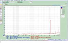
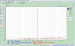
Attached is an FFT plot of my discrete DAC design, 0dB (4Vrms balanced (2.15Vrms SE)) 64K FFT, 25 AVG.
The design uses a 2 element 1Bit DAC array, operating at SDM256.
I use an Array PSU circuit based on the AD744 (FET input but somewhat noisy) with external power stage. the output opamp is a discrete DIFF opamp using 4x pairs of BC846 transistors in the input Diff pair - this measured about 2dB nosier then the OPA1632 - the Awtd dynamic range reduced to about -126dB (-128dB with the OPA1632).
0dB 997Hz 48KHz LcH DevDAC.jpg
The DAC is powered from 5V, so I'm limited by the PSU rails (+/- 5.5V) when swinging 2.15Vrms per phase the discrete opamp approaches saturation due to the limited DC supply rails at the single peaks... I believe this results in the "High" 3rd harmonic at -120dB at 0dB FS.
Whats really interesting is to compare a 2 Element (2 tap) design verses your 48 tap design
")
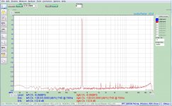
I'm now considering to push the PSU rails to give me more DC headroom for the analogue stage
I want to see harmonics around -130dB as on your design Interesting my THD is 0.0001% same as yours - but you have lower harmonics so I don't understand...
Also, my 20KHz noise floor is trending downwards, this is a result of the noise floor of the Array PSU and Opamp noise, I really need a lower noise input stage - the noise of Quad pairs of paralleled BC846's is just not low enough..
Last edited:
probably opposite phase
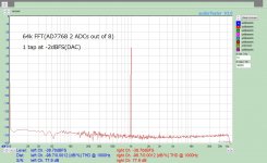
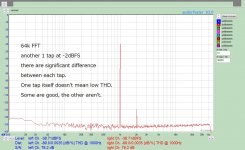
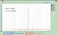
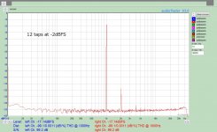
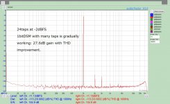
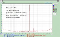
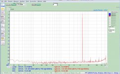
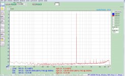
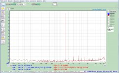
I guess low THD comes from the fortunate opposite phase between taps because each tap doesn't have excellent performance: some are good; some aren't. The attached pics are 1 tap, another 1 tap, 4taps, 12taps, 24taps, and 48taps at -2dBFS(8Vpp); tap change is controlled by the registers in the FPGA, no HW change exists. The 1st one is almost no THD, but the 2nd has some. 4 taps and 12 taps are still ordinary performance. You can have significant improvement at 24taps(the 1st booster): more than 12dB improvement. You have an additional bonus at 48taps: another more than 10dB increase(the 2nd one).
Only one possibility is the answer, IMHO. Each tap has a lucky coincidence; their harmonics(mainly 2nd and 3rd) fade away due to the opposite phase. I guess a small number(less than 12) can't make the best of the opposite phase(not enough taps to average harmonics). If you have more than 24taps, averaging effect results in low THD, like SNR improvement with paralleling. Discrete implementation isn't so stable. Even a FET probe(1 pf) can change THD value; monolithic is better. But you have a repeatable number after 10-minute warming up as long as FPGA data and PCB are the same.
I don't know the reason why each tap can totally have the opposite phase. What I know is the fast phase shift with subtle switching pulse difference. Each tap can't have an exact switching pulse phase. There can be a lucky area where fast harmonics phase change without degradation occur. I guess you can control the harmonics phase change if you are in a monolithic world. Discrete depends on lucky coincidence, one FPGA routing out of five trials.
I guess low THD comes from the fortunate opposite phase between taps because each tap doesn't have excellent performance: some are good; some aren't. The attached pics are 1 tap, another 1 tap, 4taps, 12taps, 24taps, and 48taps at -2dBFS(8Vpp); tap change is controlled by the registers in the FPGA, no HW change exists. The 1st one is almost no THD, but the 2nd has some. 4 taps and 12 taps are still ordinary performance. You can have significant improvement at 24taps(the 1st booster
): more than 12dB improvement. You have an additional bonus at 48taps: another more than 10dB increase(the 2nd one). Only one possibility is the answer, IMHO. Each tap has a lucky coincidence; their harmonics(mainly 2nd and 3rd) fade away due to the opposite phase. I guess a small number(less than 12) can't make the best of the opposite phase(not enough taps to average harmonics). If you have more than 24taps, averaging effect results in low THD, like SNR improvement with paralleling. Discrete implementation isn't so stable. Even a FET probe(1 pf) can change THD value; monolithic is better. But you have a repeatable number after 10-minute warming up as long as FPGA data and PCB are the same.
I don't know the reason why each tap can totally have the opposite phase. What I know is the fast phase shift with subtle switching pulse difference. Each tap can't have an exact switching pulse phase. There can be a lucky area where fast harmonics phase change without degradation occur. I guess you can control the harmonics phase change if you are in a monolithic world. Discrete depends on lucky coincidence, one FPGA routing out of five trials.
Attachments
I guess low THD comes from the fortunate opposite phase between taps because each tap doesn't have excellent performance: some are good; some aren't. The attached pics are 1 tap, another 1 tap, 4taps, 12taps, 24taps, and 48taps at -2dBFS(8Vpp); tap change is controlled by the registers in the FPGA, no HW change exists. The 1st one is almost no THD, but the 2nd has some. 4 taps and 12 taps are still ordinary performance. You can have significant improvement at 24taps(the 1st booster
Only one possibility is the answer, IMHO. Each tap has a lucky coincidence; their harmonics(mainly 2nd and 3rd) fade away due to the opposite phase. I guess a small number(less than 12) can't make the best of the opposite phase(not enough taps to average harmonics). If you have more than 24taps, averaging effect results in low THD, like SNR improvement with paralleling. Discrete implementation isn't so stable. Even a FET probe(1 pf) can change THD value; monolithic is better. But you have a repeatable number after 10-minute warming up as long as FPGA data and PCB are the same.
I don't know the reason why each tap can totally have the opposite phase. What I know is the fast phase shift with subtle switching pulse difference. Each tap can't have an exact switching pulse phase. There can be a lucky area where fast harmonics phase change without degradation occur. I guess you can control the harmonics phase change if you are in a monolithic world. Discrete depends on lucky coincidence, one FPGA routing out of five trials.
I suspect the Second order THD is a result of matching with the Diff pair transistors used in each DAC element...
I'm trying to find the cause of my "high" 3rd order component...
@xx3stksm: Hi again ... & thanks for posting your measurements on silence & "tutti" in #236 the other day. I really do find it interesting to see how the noise floor changes when the various DAC setups processes data signals.
One practical question in this context: How do you generate those 32 sine waves that you use? I use wave gene (kindly freely supplied by one of your countrymen I believe) but it is only capable of 8 simultaneous sine waves (as far as I know). It would be interesting to test my DAC with more sine waves, if possible ...
@#243: Now I am a bit unsure of what "one tap" is but I suppose it is one line output from the FPGA going into discrete circuitry ... ? Correct? If this is so could one explanation for the various harmonics' levels be that the components are not placed entirely in the same positions for each tap so that there are EMR variations - or small component+trace variations? The harmonics' levels are quite low so I am thinking that at these levels component placement might also have a say ... Just a thought.
Thanks again for sharing this xx3stksm ... & have a good day ;-)
Jesper
I suspect the Second order THD is a result of matching with the Diff pair transistors used in each DAC element...
I'm trying to find the cause of my "high" 3rd order component...
The 6th pic(48 taps) at #243 has almost -135dBFS 2nd harmonic while the 5th(24 taps) has -126dBFS. So, the other 24 taps must be -129dBFS with the opposite phase to have -135dBFS; the addition of two 24 taps is equal to 48 taps. I'm sure it's the only answer to have -135dBFS in 48 taps. The 3rd harmonic of the other 24 taps is almost the same amplitude with the opposite phase to achieve -150dBFS.
@xx3stksm: Hi again ... & thanks for posting your measurements on silence & "tutti" in #236 the other day. I really do find it interesting to see how the noise floor changes when the various DAC setups processes data signals.
One practical question in this context: How do you generate those 32 sine waves that you use? I use wave gene (kindly freely supplied by one of your countrymen I believe) but it is only capable of 8 simultaneous sine waves (as far as I know). It would be interesting to test my DAC with more sine waves, if possible ...
@#243: Now I am a bit unsure of what "one tap" is but I suppose it is one line output from the FPGA going into discrete circuitry ... ? Correct? If this is so could one explanation for the various harmonics' levels be that the components are not placed entirely in the same positions for each tap so that there are EMR variations - or small component+trace variations? The harmonics' levels are quite low so I am thinking that at these levels component placement might also have a say ... Just a thought.
Thanks again for sharing this xx3stksm ... & have a good day ;-)
Jesper
Yes, I made a 32-tone file with Wave Gen. It's incredible it has a very fine resolution, 99.609375Hz,999.0234375Hz, and 20000.9765625Hz. If you want more than eight sinewaves(32-tone), you need to have four groups: 4*(8-tone). You can add them together with editing SW, like RX7.
Mine is here. You can download it. See the attached pic.
Yahoo!ボックス - 大切な思い出をずっと大事にお預かりします
You are correct as to the meaning of one tap. The taps have some variations because of track length, switching pulse phase, temperature, and resistor tolerance. Their diversity sometimes for you or against you. I need to have some FPGA routing trials to achieve a good result. Once you have found the excellent routing, it can be partially used for the next routing: accumulation is possible.
Attachments

@xx3stksm ... Many thanks for the file. I will check it in the days to come (might be Monday or Sunday) and maybe - if I dare so  - post my results here.
WRT heating on your PCB ... I remember you use very small transistors: Might adding a substance similar to the material the transistors are made from onto the individual transistors help improve thermal (and maybe vibrational) stability on your PCB?
Cheers,
Jesper
- post my results here.WRT heating on your PCB ... I remember you use very small transistors: Might adding a substance similar to the material the transistors are made from onto the individual transistors help improve thermal (and maybe vibrational) stability on your PCB?
Cheers,
Jesper
Attached is an FFT plot of my discrete DAC design, 0dB (4Vrms balanced (2.15Vrms SE)) 64K FFT, 25 AVG.
The design uses a 2 element 1Bit DAC array, operating at SDM256.
I use an Array PSU circuit based on the AD744 (FET input but somewhat noisy) with external power stage. the output opamp is a discrete DIFF opamp using 4x pairs of BC846 transistors in the input Diff pair - this measured about 2dB nosier then the OPA1632 - the Awtd dynamic range reduced to about -126dB (-128dB with the OPA1632).
THATcorp 300 series BJT arrays are an alternative for the IP dif pairs on
discrete OPA's if you want to get the noise right down (<= 1nV/rt Hz) but still
maintain low Cob and high ft = 350MHz.
In fact these arrays might also be very good for the actual bit current sources
(if you are using current sources as opposed to just logic switched resistors.)
Are you using RTZ encoding on these DAC's?
I was thinking / plotting an RTZ coding scheme the other day to equalize the non perfect 'edge energy' but started to delve into ways to cancel noise floor
modulation with similar coding. But i'm no expert on these things, just creative thinking.
The DAC is powered from 5V, so I'm limited by the PSU rails (+/- 5.5V) when swinging 2.15Vrms per phase the discrete opamp approaches saturation due to the limited DC supply rails at the single peaks... I believe this results in the "High" 3rd harmonic at -120dB at 0dB FS.
I'm now considering to push the PSU rails to give me more DC headroom for the analogue stage
IME, once you squash rails down and push voltage swing close to rails on discrete designs, voltage modulated Cob really starts to work against low
distortion. Higher rails + pulling a few tricks like running more OP bias, two pole compensation and even utilizing the 'Jensen 990' degenerated IP pair
can be an advantage over chips.
Interesting my THD is 0.0001% same as yours - but you have lower harmonics so I don't understand...
Is the distortion from the 1 bit DAC array or is it from the analog OP stage.
Ltspice can come in handy to help hone these designs.
TCD
THATcorp 300 series BJT arrays are an alternative for the IP dif pairs on
discrete OPA's if you want to get the noise right down (<= 1nV/rt Hz) but still
maintain low Cob and high ft = 350MHz.
Terry,
Cost is an issue with THATcorp - Cob is not an issue in this design due to the very low array source impedance. Its just cheaper to parallel BC846's, really I should have used PNP's but I also wanted to offer the choice to use FET devices, and for that I really need to use Nchannel parts in the same location with small component value tweaks in the circuit.
In fact these arrays might also be very good for the actual bit current sources (if you are using current sources as opposed to just logic switched resistors.)
As I require lowest output impedance, I'm using "logic switch resistor" - its a modern day spin on my first discrete designs from early 90's (used in such designs as the Pink Triangle DaCapo etc).
Are you using RTZ encoding on these DAC's?
I was thinking / plotting an RTZ coding scheme the other day to equalize the non perfect 'edge energy' but started to delve into ways to cancel noise floor
modulation with similar coding. But i'm no expert on these things, just creative thinking.
Yes, using balanced RTZ encoding, going fully balanced largely removes the issue of unequal edge energy.
, once you squash rails down and push voltage swing close to rails on discrete designs, voltage modulated Cob really starts to work against low distortion.
Everything's "bootstrapped" Cascoded in the design so I dont see Cob modulation - requiring the extra voltage headroom for Cascoding with such low rail voltage is a real challenge.
Higher rails + pulling a few tricks like running more OP bias, two pole compensation and even utilizing the 'Jensen 990' degenerated IP pair can be an advantage over chips.
Sure, but I dont have the luxury of higher supply rails (atleast on this PCB spin)... whats the 'Jensen 990' degenerated IP pair is it different from standard Emitter degeneration?
I find complex feedback compensation sounds worst - its become more about achieving technical performance numbers then sonic performance. With a few mods, the THD is now below -120dB at full-scale (rapidly dropping below -130dB at a little lower output levels).
Is the distortion from the 1 bit DAC array or is it from the analog OP stage.
I suspect its more due to the Analogue stage then DAC array ATM - I'll increase the size of the DAC array on the next PCB spin, also most likely move away from being USB self-powered and then can increase the Analogue supply rails.
Ltspice can come in handy to help hone these designs.
For sure I use spice, there is no way I could reliably design such complex circuits without it, however its my experience that spice does not give absolute distortion figures at such low levels - spice is a useful tool to determine the "direction" of THD etc but your at the mercy of model accuracy / circuit parasitics at these super low THD levels...
Last edited:
WRT cost, thought you might say that.Terry,
Cost is an issue with THATcorp - Cob is not an issue in this design due to the very low array source impedance. Its just cheaper to parallel BC846's, really I should have used PNP's but I also wanted to offer the choice to use FET devices, and for that I really need to use Nchannel parts in the same location with small component value tweaks in the circuit.
If Cob is not an issue, if there is a SMD version of the BC337 type process,
the noise is less than half of 846 family.
So effectively the OP of each bit looks like a pulse train, each pulse having a finite and exactly repeatable amount of energy, the linearity mainly only restricted by timing accuracy and PS fluctuations.Yes, using balanced RTZ encoding, going fully balanced largely removes the issue of unequal edge energy.
In these cases 1/2 V can make a significant difference to move the operating point away from the 'knee'. I must admit I am lazy in this regard and have rarely designed anything within super constrained voltage rails. Usually it's the opposite.Everything's "bootstrapped" Cascoded in the design so I dont see Cob modulation - requiring the extra voltage headroom for Cascoding with such low rail voltage is a real challenge.
Jensen 990Sure, but I dont have the luxury of higher supply rails (atleast on this PCB spin)... whats the 'Jensen 990' degenerated IP pair is it different from standard Emitter degeneration?
https://www.google.com.au/url?sa=t&.../pdf/990.pdf&usg=AOvVaw0YT5grNhDOglbS5qqI87PJ
Weiss OP1 uses same
https://www.weiss.ch/files/downloads/op1-bp/OP1-BP-Datasheet-R1.pdf
I haven't got to the bottom of that yet. Currently playing with a CFB, fully balanced power amp that has various implementations of TPC or not.I find complex feedback compensation sounds worst - its become more about achieving technical performance numbers then sonic performance. With a few mods, the THD is now below -120dB at full-scale (rapidly dropping below -130dB at a little lower output levels).
Distortion is lower but bode plot says there is 'illegal' phase margin at lower frequencies. It won't oscillate but exactly how does that affect sound?
Well, I guess you just solved your own problem WRT PS rails / opamp.I suspect its more due to the Analogue stage then DAC array ATM - I'll increase the size of the DAC array on the next PCB spin, also most likely move away from being USB self-powered and then can increase the Analogue supply rails.
For sure I use spice, there is no way I could reliably design such complex circuits without it, however its my experience that spice does not give absolute distortion figures at such low levels - spice is a useful tool to determine the "direction" of THD etc but your at the mercy of model accuracy / circuit parasitics at these super low THD levels...
Depending on circuit and models, Spice seems to be pretty good to low
0.000x% numbers, maybe a little better but beyond that I think it is a really good tool for giving insight into the mechanisms at play.
TCD
Hi ... just a brief update to my #248 comment about measuring my DAC with the sine waves xx3stksm kindly provided (I prefer to follow-up on things I say even if it may be of less importance here): I won't have time for it right now but will do so when time becomes available ... ...
Cheers,
Jesper
Cheers,
Jesper
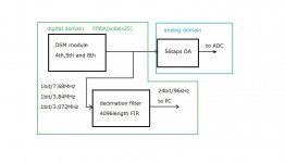
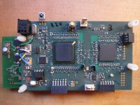
It has been a long time since the last update. I revised PCB(4th edition) last September to fix some remaining problems, repeatability, out-of-band noise, and power consumption. Pic.1 is the final version, which has 2 FPGAs(xc6slx25 and xc6slx9). A small PCB on the left side is due to heat problem. If regulators are on the main PCB, the left side becomes a bit warmer than the rest, which leads to unequal temperature conditions. xc6slx25 includes over-sampling filters, DSM, and 30taps, while xc6slx9 has 26taps only, without a complicated circuit. xc6slx25 physically can have 56taps but ends up less SNR. xc6slx9 for shift resisters only is the point to have excellent repeatability. BGA is also better than QFP if you want high SNR because it has more power and GND pins than QFP though it's impossible to do hand soldering.
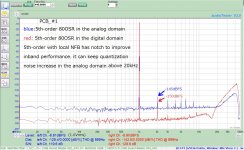
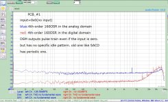
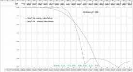
Pic.2 is FFT, where blue is the performance in the analog domain and red is in the digital. The digital domain's performance is the decimation filter's output (4096taps), converting 1bitDSM into 24bit/96kHz(pic. 3 and pic. 4). It's convenient to estimate DAC quality if you have digital domain FFT. The difference between the analog and the digital means how much your 1bitDSM DAC is off from the ideal DAC.
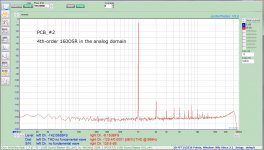
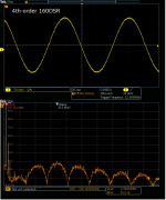
Pic.5 is the small amplitude(0.1Vrms) waveform and out-of-band FFT(up to 1MHz). I employ 4th-order in 160OSR instead of 256OSR. High OSR can have good noise-shaping performance while it tends to end up with low SNR. I'm sure 160OSR is the best point for my HW(48000x160=7.68MHz). Pic.6 is idling pattern. When the input is zero, old DSM sometimes outputs unexpected noise pattern.The recent one gets rid of the specific idle pattern with an almost flat FFT.
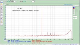
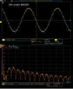
Another improvement with the 4th PCB is to make the best of 5th-order in 80OSR. Generally speaking, the lower OSR, the better THD because low OSR means less toggling. If you use 80OSR, 6th-order is enough but a little bit overkill. 5th-order in 80OSR usually can't have excellent SNR due to poor noise-shaping performance. I have successfully tweaked 5th-order DSM so that SNR degradation is acceptable while maintaining high THD(Pic. 7 and pic.8). Out-of-band noise is a bit larger than 4th-order.
I have already soldered and adjusted 4 PCBs. They are almost the same performance as pic.2. In other words, they can be the same. What I need to do is to find an optimum combination to achieve the goal. The combination doesn't mean analog adjustment like resistor matching but digital ones that are to be stored into registers. Pic.9 and pic.10 are another PCB, which is probably the best in 4PCBs. High repeatability guarantees such excellent performance after five minutes of warming up. Five minutes is necessary to average transistors' temperature. It takes about two years before I have almost finished designing and implementing 1bit DSM for my personal use. Neither short nor long.
I revised PCB(4th edition) last September to fix some remaining problems, repeatability, out-of-band noise, and power consumption. Pic.1 is the final version, which has 2 FPGAs(xc6slx25 and xc6slx9). A small PCB on the left side is due to heat problem. If regulators are on the main PCB, the left side becomes a bit warmer than the rest, which leads to unequal temperature conditions. xc6slx25 includes over-sampling filters, DSM, and 30taps, while xc6slx9 has 26taps only, without a complicated circuit. xc6slx25 physically can have 56taps but ends up less SNR. xc6slx9 for shift resisters only is the point to have excellent repeatability. BGA is also better than QFP if you want high SNR because it has more power and GND pins than QFP though it's impossible to do hand soldering. Pic.2 is FFT, where blue is the performance in the analog domain and red is in the digital. The digital domain's performance is the decimation filter's output (4096taps), converting 1bitDSM into 24bit/96kHz(pic. 3 and pic. 4). It's convenient to estimate DAC quality if you have digital domain FFT. The difference between the analog and the digital means how much your 1bitDSM DAC is off from the ideal DAC.
Pic.5 is the small amplitude(0.1Vrms) waveform and out-of-band FFT(up to 1MHz). I employ 4th-order in 160OSR instead of 256OSR. High OSR can have good noise-shaping performance while it tends to end up with low SNR. I'm sure 160OSR is the best point for my HW(48000x160=7.68MHz). Pic.6 is idling pattern. When the input is zero, old DSM sometimes outputs unexpected noise pattern.
The recent one gets rid of the specific idle pattern with an almost flat FFT.Another improvement with the 4th PCB is to make the best of 5th-order in 80OSR.
Generally speaking, the lower OSR, the better THD because low OSR means less toggling. If you use 80OSR, 6th-order is enough but a little bit overkill. 5th-order in 80OSR usually can't have excellent SNR due to poor noise-shaping performance. I have successfully tweaked 5th-order DSM so that SNR degradation is acceptable while maintaining high THD(Pic. 7 and pic.8). Out-of-band noise is a bit larger than 4th-order.I have already soldered and adjusted 4 PCBs. They are almost the same performance as pic.2. In other words, they can be the same. What I need to do is to find an optimum combination to achieve the goal. The combination doesn't mean analog adjustment like resistor matching but digital ones that are to be stored into registers. Pic.9 and pic.10 are another PCB, which is probably the best in 4PCBs. High repeatability guarantees such excellent performance after five minutes of warming up. Five minutes is necessary to average transistors' temperature. It takes about two years before I have almost finished designing and implementing 1bit DSM for my personal use. Neither short nor long.
Attachments
-
 5th_2x.jpg292.4 KB · Views: 148
 -
 4th_2x.jpg294.4 KB · Views: 145
 -
 20210306231300.png22.4 KB · Views: 141
 -
 56tap_5th.jpg345.6 KB · Views: 130
 -
 56tap_idle.jpg330.3 KB · Views: 137
 -
 20210306224740.png22.1 KB · Views: 371
 -
 4096FIR.jpg274.9 KB · Views: 365
 -
 _schema.jpg105.9 KB · Views: 402
 -
 56tap_4th.jpg343.7 KB · Views: 388
 -
 IMG_5761.jpg1,000.9 KB · Views: 400
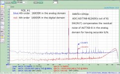
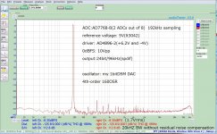
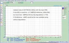
It's challenging to have an ADC with high THD performance and low noise floor. My current ADC chip is AD7768-8, which can have -130dB THD.
https://www.analog.com/media/en/technical-documentation/application-notes/AN-1384.pdf
Residual noise depends on the numbers of ADC(up to 8) and a reference voltage. The larger a reference voltage(up to 6V), the lower the noise floor. I'm sure you need to have two setups; one for THD and the other for SNR. An ADC for THD can't have an excellent noise floor because a reference voltage is 4V at max for accurate THD. A practical solution is software simulation. An ADC for SNR(paralleling 8 ADCs) measures the noise floor of DUT. Then you compensate the noise floor of an ADC for THD with SW. There may be a 1dB error in absolute value but enough for a DIYer. THD is probably correct.
No problem, my motto is "no ADC, no DAC. " it's not easy to have an AP product for a DIYer. But DAC performance is in proportion to ADC, especially if THD is beyond -120dB. AD7768-8 is probably reliable because each of them(8 ADCs) has almost the same THD performance. THD measured by one ADC and by two ADCs have no difference. THD over frequency is a bit tricky because my DAC accepts an optimized optical signal fed by transport or ADC. Both only have limited frequencies for practical use. They are 187Hz,375Hz,750Hz,999Hz,1.5kHz,3kHz,6kHz and 12kHz(999Hz=(96000/32768)*341) from pic.1 to pic8. The max swing is 10Vpp(differential) but -3dBFS(7Vpp) is practically max amplitude. If your DAC has more than 7Vpp, you need to have a resistor divider.
The noise floor of them isn't compensated. You can compensate the value with the residual noise of two ADCs(-120.3dBFS, pic.9) though there may be some error. If you use 8 ADCs, you can have -127dBFS residual noise, where more accurate than 2 ADCs.
" it's not easy to have an AP product for a DIYer. But DAC performance is in proportion to ADC, especially if THD is beyond -120dB. AD7768-8 is probably reliable because each of them(8 ADCs) has almost the same THD performance. THD measured by one ADC and by two ADCs have no difference. THD over frequency is a bit tricky because my DAC accepts an optimized optical signal fed by transport or ADC. Both only have limited frequencies for practical use. They are 187Hz,375Hz,750Hz,999Hz,1.5kHz,3kHz,6kHz and 12kHz(999Hz=(96000/32768)*341) from pic.1 to pic8. The max swing is 10Vpp(differential) but -3dBFS(7Vpp) is practically max amplitude. If your DAC has more than 7Vpp, you need to have a resistor divider. The noise floor of them isn't compensated. You can compensate the value with the residual noise of two ADCs(-120.3dBFS, pic.9) though there may be some error. If you use 8 ADCs, you can have -127dBFS residual noise, where more accurate than 2 ADCs.
Attachments
@xx3stksm: IMHO very impressive results you have reached with your DAC ... I am thinking that it would indeed have been interesting to listen to it (if possible, of course) but, well, Japan is somewhat distant not least in these covid-19 times ... 
Also, seeing what you can accomplish with FPGA programming really makes me wish that I was able to program but at least currently no time to learn it ...
Just two questions in relation to your ADC: I suppose that the reason why you may not use a notch filter in front of your ADC is that you may also want to use the multi-frequency test signal that you have mentioned earlier in this thread, right? And specifically in relation to the ADC: Is it one you have designed yourself or are you using the evaluation boards from Analog Devices?
Cheers from Denmark,
Jesper M
A P.S.: Regarding the multi-frequency signal file you kindly posted a download link to some time ago. I have to admit that I have not yet had the time to try it out as life has been very busy indeed. My apology for this. However, in the meantime I have also decided that I will re-design this DAC and I hope to use e.g. your test method in this context as it appears to be very useful.
Also, seeing what you can accomplish with FPGA programming really makes me wish that I was able to program
but at least currently no time to learn it ...Just two questions in relation to your ADC: I suppose that the reason why you may not use a notch filter in front of your ADC is that you may also want to use the multi-frequency test signal that you have mentioned earlier in this thread, right? And specifically in relation to the ADC: Is it one you have designed yourself or are you using the evaluation boards from Analog Devices?
Cheers from Denmark,
Jesper M
A P.S.: Regarding the multi-frequency signal file you kindly posted a download link to some time ago. I have to admit that I have not yet had the time to try it out as life has been very busy indeed. My apology for this. However, in the meantime I have also decided that I will re-design this DAC and I hope to use e.g. your test method in this context as it appears to be very useful.
- Home
- Source & Line
- Digital Line Level
- My no DAC project, FPGA and transistors