The noise floor of them isn't compensated. You can compensate the value with the residual noise of two ADCs(-120.3dBFS, pic.9) though there may be some error. If you use 8 ADCs, you can have -127dBFS residual noise, where more accurate than 2 ADCs.
Hmm, I think I don't understand your graphs. Pic 9 more looks like noise floor at -150dBFS though you talk about -117dBFS. Similar for the THD graphs which seem to indicate much lower THD than your written comments. Maybe you could clarifiy on that.
Second question: Which software do you use there?
Third question: How do you convert the proprietary serial signal from the ADC to SPDIF? Do you use the evval board or did you brew your own board? Currently I'm thinking of whipping together an stm32 board that could also work as UAC2 compliant device and thus work as soundcard input under linux. But if you have a simpler solution involving the conversion to SPDIF I'd be glad to hear about it. If you want to share your intellectual property that is 🙂
Just two questions in relation to your ADC: I suppose that the reason why you may not use a notch filter in front of your ADC is that you may also want to use the multi-frequency test signal that you have mentioned earlier in this thread, right? And specifically in relation to the ADC: Is it one you have designed yourself or are you using the evaluation boards from Analog Devices?
Cheers from Denmark,
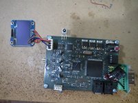
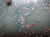
My ADC board(the attached pic) has a footprint of a notch filter. But I haven't had a good result on SNR. It's not preferable to use more than a 500ohm resistor if your target is more than 120dB SNR. Fortunately, AD7768 and TI's precise ADCs don't force you to eliminate the fundamental even if DUT has less than -130dB THD. So, I gave up a notch filter.
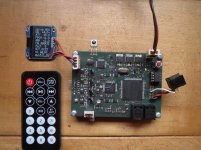
The pic is 1st version, where I had some mistakes and found some functions to add(HDMI-IIS and an optical output for DAC to do synchronous sampling). The 2nd one is now under construction to fix bugs and improve a digital process, which means a bit large FPGA(now xc6slx9) is necessary.🙂
Attachments
Have you done a three tone test with (combined) levels close to clipping? If you pass that you are good to go. Nice project!!!
//
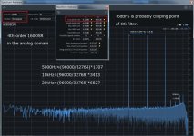
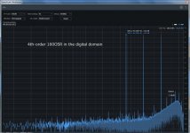
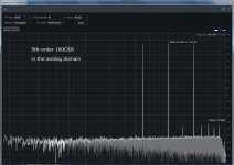
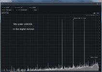
Pic.1(analog domain) and pic.2(digital domain) are three tones close to the clipping level. Distortions more than 35kHz are a bit larger than lower frequencies. I guess this is caused by less noise-shaping because the digital domain already has large ones. If you use 5th-order 160OSR(pic. 3), which has better noise-shaping, more than 35kHz are almost the same as low frequencies. Pic4(digital domain) suggests that noise-shaping is effective at 40kHz. The difference is THD loss by DA process.
Pic.5 is 32tone, the same one ASR is employing.
Topping D90 Balanced USB DAC Review | Audio Science Review (ASR) Forum
I guess their FFT size is 256k, but I don't know what windowing they use. 1bitDSM has less periodicity than a multi-bit one theoretically. Less periodicity ends up the degradation of the noise floor. It would be the disadvantage of 1bitDSM, though I don't think it's audible.
Attachments
Hmm, I think I don't understand your graphs. Pic 9 more looks like noise floor at -150dBFS though you talk about -117dBFS. Similar for the THD graphs which seem to indicate much lower THD than your written comments. Maybe you could clarifiy on that.
Second question: Which software do you use there?
Third question: How do you convert the proprietary serial signal from the ADC to SPDIF? Do you use the evval board or did you brew your own board? Currently I'm thinking of whipping together an stm32 board that could also work as UAC2 compliant device and thus work as soundcard input under linux. But if you have a simpler solution involving the conversion to SPDIF I'd be glad to hear about it. If you want to share your intellectual property that is 🙂
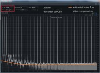
If you want to calculate the noise power of pic.9, the FFT bin and bandwidth are necessary. FFTbin=sampling freq/FFT size=96000/65536=1.46. The noise power is the square root sum of the bin from 0 to 20kHz(BW=20kHz). If the bin is -160dB,rough estimation is
noise power=-160+10*log(20000/1.46)=-118.7dBFS.
The audio Tester does the accurate value. -120.32dBFS is probably correct, though a 1dB error can exist(RX7 outputs a bit different value).
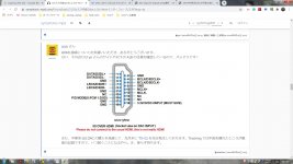
ADC output(quasi 192kHz SPI) goes to FPGA(xc6slx9), then FPGA outputs spdif(24bit/96kHz), HDMI-IIS(up to 32bit/192kHz) and optical interface(phase modulation). The LPC1347(cortex-M3) controls FPGA registers and OLED via IR. If you want to control the ADC from Linux, some interface like IIC is simple. Another option is HAT. Rpi can directly accept IIS, though I have not experienced IIS output. Rpi has IIC.
I'm now designing the next version of my ADC. Some modification is possible to be compatible with your needs. But it's not easy for a DIYer to solder 1005 chips as close to power and GND pins as possible. You could have a short-circuit. I can share PCB data(Garber) and FPGA data(MCS) but can't provide a populated PCB.
Attachments
@xx3stksm: Thanks again for your feedback ... hmmm ... impressive that you have reached these results with the ADC. And again makes me think that it would have been great to be able to program an FPGA - I reckon it would open up a world of DIY options (when it had been learned thoroughly)!
WRT a notch filter I see your point with the SNR ... I am thinking though that one way to have both the advantage of the notch filter in terms of THD measurements and SNR could be to make the notch filter switchable ON/OFF - while still keeping the notch resistances low so as to not swamp the ADC with the notch filter's noise.
Thanks again for sharing xx3stksm ;-)
Cheers,
Jesper
If you want to calculate the noise power of pic.9, the FFT bin and bandwidth are necessary. FFTbin=sampling freq/FFT size=96000/65536=1.46. The noise power is the square root sum of the bin from 0 to 20kHz(BW=20kHz). If the bin is -160dB,rough estimation is
noise power=-160+10*log(20000/1.46)=-118.7dBFS.
The audio Tester does the accurate value. -120.32dBFS is probably correct, though a 1dB error can exist(RX7 outputs a bit different value).
Thanks very much for the detailed explanation!
ADC output(quasi 192kHz SPI) goes to FPGA(xc6slx9), then FPGA outputs spdif(24bit/96kHz), HDMI-IIS(up to 32bit/192kHz) and optical interface(phase modulation). The LPC1347(cortex-M3) controls FPGA registers and OLED via IR. If you want to control the ADC from Linux, some interface like IIC is simple. Another option is HAT. Rpi can directly accept IIS, though I have not experienced IIS output. Rpi has IIC.
I'm now designing the next version of my ADC. Some modification is possible to be compatible with your needs. But it's not easy for a DIYer to solder 1005 chips as close to power and GND pins as possible. You could have a short-circuit. I can share PCB data(Garber) and FPGA data(MCS) but can't provide a populated PCB.
Thanks again for this generous offer!
I'm currently designing the "motherboard" for our 10 channel DAC project. This will have the clock distribution, an XMOS with 5 I²S outputs, a CP2112 USB/I²C bridge and an 8 channel I²S multiplexer on board. 6 of the I²S channels are already in use for the DAC chips and the clock divider. So I have 2 spare, one possibly for the ADC. The XMOS also receives the MCLK (22.5792/24.576) via optoisolator so everything can run in full synchronous mode. All signals are distributed over HDMI cables to the DAC boards.
If we could integrate your ADC board into this setup, possibly by sending the MCLK and I²S BCK/LRCK back to your board and receiving I²S DATA to feed it to the XMOS, that would be marvelous!!! I don't know how much redesign is necessary on your side to be able to receive BCK/LRCK to act as a slave instead of generating them. Maybe the idea is not feasible at all, you will have to tell me.
If this cannot work we would still be glad to try and build your board and use the spdif via some USB interface into linux.
On the topic of soldering 1005 caps - that will be a huge challenge, but we would certainly try. We have an oven for soldering though the smallest resistor we soldered so far was 0603. 1005 is a completely different league...
If we could integrate your ADC board into this setup, possibly by sending the MCLK and I²S BCK/LRCK back to your board and receiving I²S DATA to feed it to the XMOS, that would be marvelous!!! I don't know how much redesign is necessary on your side to be able to receive BCK/LRCK to act as a slave instead of generating them. Maybe the idea is not feasible at all, you will have to tell me.
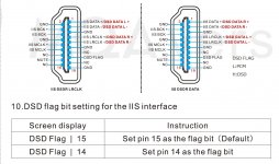
If your motherboard can output MCLK and LRCK via HDMI-IIS(LVDS), it's straightforward to use them to do synchronous sampling. Then my ADC board outputs DATA to your motherboard. My FPGA configuration will use HDMI-IIS as outputs(MCLK, BCK, LRCK, and DATA). For your configuration, HDMI-IIS acts as two inputs(MCLK and LRCK from your motherboard, BCK is don't care) and one output(DATA). PCB layout needs no change. Only configuration data(MCS) is different.How about controlling FPGA registers, which can change ADC's sampling frequency and power dissipation? It's possible to use IIC of HDMI-IIS. FPGA has enough I/Os to be configured as LVDS.
One concerning thing via HDMI-IIS is the voltage difference on signal GND between them if both are powered by the main(optical is completely safe). Even 5V is dangerous enough to fry FPGA. HDMI cable is usually "GND first." As long as the first contact is GND, no problem occurs. As to 1005, it means 0402😱.
Attachments
I was planing to just use 3.3V I²C over the hdmi cable for the DACs. So it would make sense to use that to control the ADC, too. That all sounds very good to me.
I am planning to use LVPECL as drive level to our DACs with a termination resistor of 100 ohms at the receiving side. Do we need to adjust levels for your ADC board to LVDS then?
I am planning to use LVPECL as drive level to our DACs with a termination resistor of 100 ohms at the receiving side. Do we need to adjust levels for your ADC board to LVDS then?
Pic.1(analog domain) and pic.2(digital domain)...
Impressive - congratulations!
//
I am planning to use LVPECL as drive level to our DACs with a termination resistor of 100 ohms at the receiving side. Do we need to adjust levels for your ADC board to LVDS then?
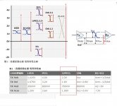
Unfortunately, FPGA doesn't support LVPECL output(input only). If the ADC board outputs LVPECL (data to your motherboard), PPDS with AC coupling is a candidate to ensure a 0.7V swing required by LVPECL. I think it's not impossible to use PPDS output instead of LVPECL. If LVPECL isn't mandatory, LVDS is easier than LVPECL.
Attachments

On the receiving (my) side I could also cope with LVDS, no problem. If your ADC board can cope with LVPECL then that is sweet as then don't have to use different sender ICs.
Very nice. Your ADC project now just got our favourite option! 🙂
One more questions: What HW tools are needed to program the MCU and the FPGA?
One more questions: What HW tools are needed to program the MCU and the FPGA?
A standard SPI EEPROM(25 families) is better than a specialized one to store FPGA configuration data because they are inexpensive. JTAG cable is also a bit expensive($60 by Diligent). I usually use A25L080-F or SST25VF080B-50-4C-PAE and an ordinary ROM writer(SmartProv2). In some cases, even four JTAG wires are difficult to route. If you don't have a ROM writer, you can find a USB programmer on eBay.
USB Programmer CH341A Series Burner Chip 24 EEPROM BIOS Writer 25 SPI Flash h3 | eBay
You don't need to program MCU(Cortex-M3) because you can access ADC registers via IIC. MCU and IIC(HDMI-IIS) are mutually exclusive. You don't need to populate MCU.
USB Programmer CH341A Series Burner Chip 24 EEPROM BIOS Writer 25 SPI Flash h3 | eBay
You don't need to program MCU(Cortex-M3) because you can access ADC registers via IIC. MCU and IIC(HDMI-IIS) are mutually exclusive. You don't need to populate MCU.
@xx3stksm: Hmmm ... If possible I would appreciate your comment on this new ADC from Analog, the AD7134, and in particular its evaluation board which can be found here:
EVAL-AD7134FMCZ Evaluation Board | Analog Devices
That is what do you think of it - particularly in terms of likely sound quality (I will modify/alter the input stage etc.)?
It is interesting to me because it will allow for simultaneous recording of up to 8 channels at an apparently very high quality (THD < 120 dB) as well as a high sampling rate (as you may remember I prefer this).
Also, I can see that it is based on continuous-time-sigma-delta sampling which, to my memory from my reading parts of Richard Schreier's "Understanding Delta-Sigma Data Converters" years ago, may be more susceptible to jitter issues than discrete time sampling (i.e. if I remember correctly). On the other hand, this may also mean that it could benefit from a HQ oscillator ...
Anyway ... Have you seen that this ADC is now available, and if so, might I ask you what you think of it?
@Tfive: Might I also ask you a question in relation to the AD7134 and something you wrote in a previous post? If so it is related to your comment:
Can I ask you if you think that this could also somehow be done for something like the hardware/software used for the EVAL-AD7134FMCZ board? The EVAL-AD7134FMCZ needs to go together with the SDP-H1 board - which is a platform board that connects many different converter boards to the PC via USB2.
The idea is to make the files sampled by the EVAL-AD7134FMCZ be recognised as "sound files" so that they may readily be entered into a recording/editing software be it Linux or Windows based ...
Now, I hope these are not too time consuming questions, yet I would appreciate your input about this ...
Cheers & thanks,
Jesper
A P.S. which is also a possible caveat: The Eval board uses a 48 MHz oscillator to allow for up to 1496 kHz sampling rates. This would - likely - have to be changed to a 49.28 MHz oscillator frequency to allow for 1.536 MHz sampling. I do not know if this is possible with the SDP-H1 board etc. transmission to the PC ... so unfortunately I reckon this is a possible caveat ...
EVAL-AD7134FMCZ Evaluation Board | Analog Devices
That is what do you think of it - particularly in terms of likely sound quality (I will modify/alter the input stage etc.)?
It is interesting to me because it will allow for simultaneous recording of up to 8 channels at an apparently very high quality (THD < 120 dB) as well as a high sampling rate (as you may remember I prefer this).
Also, I can see that it is based on continuous-time-sigma-delta sampling which, to my memory from my reading parts of Richard Schreier's "Understanding Delta-Sigma Data Converters" years ago, may be more susceptible to jitter issues than discrete time sampling (i.e. if I remember correctly). On the other hand, this may also mean that it could benefit from a HQ oscillator ...
Anyway ... Have you seen that this ADC is now available, and if so, might I ask you what you think of it?
@Tfive: Might I also ask you a question in relation to the AD7134 and something you wrote in a previous post? If so it is related to your comment:
that could also work as UAC2 compliant device and thus work as soundcard input under linux
Can I ask you if you think that this could also somehow be done for something like the hardware/software used for the EVAL-AD7134FMCZ board? The EVAL-AD7134FMCZ needs to go together with the SDP-H1 board - which is a platform board that connects many different converter boards to the PC via USB2.
The idea is to make the files sampled by the EVAL-AD7134FMCZ be recognised as "sound files" so that they may readily be entered into a recording/editing software be it Linux or Windows based ...
Now, I hope these are not too time consuming questions, yet I would appreciate your input about this ...
Cheers & thanks,
Jesper
A P.S. which is also a possible caveat: The Eval board uses a 48 MHz oscillator to allow for up to 1496 kHz sampling rates. This would - likely - have to be changed to a 49.28 MHz oscillator frequency to allow for 1.536 MHz sampling. I do not know if this is possible with the SDP-H1 board etc. transmission to the PC ... so unfortunately I reckon this is a possible caveat ...
Last edited:
I only briefly looked at the SDP-H1 manual and they don't state which format is used for the USB connection to the PC. I would assume it's a proprietary protocol and not UAC2. I'd suggest you ask AD about this. If you find out something, please post it here.
If you want to make these ADC work with an XMOS interface you have to convert the serial protocol on the ADC's output to I2S, which is what xx3stksm's board does in the FPGA.
If you want to make these ADC work with an XMOS interface you have to convert the serial protocol on the ADC's output to I2S, which is what xx3stksm's board does in the FPGA.
The AD7134 is probably one of the flagship chips of AD's DSM ADC. The AD7134 can have 1496kps sampling, though available BW depends on your acceptable RMS noise. You can have excellent performance up to 384kps; no quantization noise increase, while the AD7768 is up to 256kps. My AD7768 ADC board is also capable of both 256kps and 192kps. But I haven't had the difference between them(256kps is converted into 96kHz by SSRC). If you compare them in the same BW(20kHz or 40kHz), there's no difference. I guess they are the same architecture.
The AD7134 is more user-friendly because it includes internal logic to average four ADCs for process gain. But if you use them for an audio interface, 44.1k family or 48k family is mandatory. Other functions such as an external clock,spdif, and HDMI-IIS(for synchronous operation) are necessary. That's why even if the AD7134 includes some useful functions, having FPGA is the best solution. If your target must have 384kps, the AD7134 is the best candidate, cutting-edge, and inexpensive(less than $40).
SDP-H1 is the motherboard for many AD's ADC chips. AD7768 EV board also works in conjunction with it. The attached SW with EV board isn't cool, far behind the standard application. It's only for measurement purposes. It must be in conjunction with FPGA and suitable SW to make the best of it.Unfortunately, the AD7134 and the AD7768 have a different footprint. It's not tricky to redesign PCB, though I guess the analog circuit must be redesign to be compatible with wide BW.
- Home
- Source & Line
- Digital Line Level
- My no DAC project, FPGA and transistors