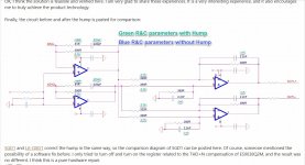
As you already know, I presume, one of the purposes of the feedback cap is to reduce the bandwidth at the converter, but it also has a second purposes: to reduce the stability damaging phase lag from the filter stage caps, at high frequency. So, as those 2 filter stages are different (i.e. 2700 pF vs. 680 pF), the feedback caps at previous stage are different.I am curious why/how the capacitor values are so different?
So I have some familiarity with how the stages go together, along with the tables and/or formulae for design. I am more curious as to why the PCM1794 filter was designed much larger capacitors (and some of the resistors are smaller, while R1 is the same) while the ES9038Q2M was much smaller capacitors (and some of the resistors are larger, while R1 is the same.) Is it nothing more than how the equations worked out for the chosen filter type? Or was BB/Ti aiming to use larger capacitors (and some smaller resistors) for a performance reason?
in IV convertors, the capacitor is also used to compensate for the (unknown) input capacitance, present at the opamp input pin. it is suggested to make it as large as possible, without encroaching on the frequencies of interest. Here, Ti is filtering harder. it is also using an older opamp that is perhaps less able to reject the HF images folded down into the audio band, thus making the LPF lower.
Each dac has different current output and noise spectrum. Ak499x, or es90xx,ADxxxx or Pcm17xx. You can"t just copy paste filter from other dacs, although all are current output or voltage output...also inner output construction...qiute a lot of known and maybe for now unknown issues.
Use this filter...it is calculated to have no thd hump. I use Transformes on output, so i didn"t tested it.
I see you do a lot of measurements...what about listening to different results... To get what you need you must do both.
Use this filter...it is calculated to have no thd hump. I use Transformes on output, so i didn"t tested it.
I see you do a lot of measurements...what about listening to different results... To get what you need you must do both.
Attachments
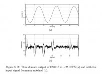
Is this the hump that you are referring to? ESS THD ‘Hump’ Investigation | Page 5 | Audio Science Review (ASR) Forum
The schematic of an output stage in post 3003 has been inspiration for various initiatives to produce a pcb. Markw4 has made a separate document with a detailed description for a board, tightly connected to the dac-pcb. I have prepared an output stage based on the board design of Daniel Green, a big Thanks. Daniel posted his gerber files, and the part numbering for his asymmetrical version (single ended part of post 3003, for rca connectors) is somewhat different to the one in post 3003. Enclosed you will find a ‘conversion’-list I made before mounting the components.
Also the Vref for two channels is ready now. All it takes is to connect the pcb to the dac v1.07. That is where a question arises, not yet addressed in this thread. Probably, those who already have made an output stage were knowledgeable enough to sort out themselves.
The four connections of the dac (dac-r, dac-rb, dac-l, dac-lb) to the original opamp are each first encountering a resistor of 6k2. Preferably, the connection to the separate dac-board is to be made by simply soldering a wire on the four resistors at the dac side, leaving the resistors in place. Then, no worry about reverse changes, keep the option of comparing the two output stages (part of the diy fun), and keep the original headphone output.
But. What will happen when two output stages are connected to the dac output? Can someone please elaborate on the possible consequences? Can they influence each other? Or if, for instance, the dac output would be burdened too much, so the four resistors might better be removed? In the approach of Markw4 even all original components of the output stage are removed.
Anyone please?
Attachments
Last edited:
Is this the hump that you are referring to?
Yes. It has been discussed multiple times in this thread, including ways to measure it and methods some people have claimed is a fix for it.
Not only is there that, but its possible to see an issue of excess heat dissipation in the IV and Summing opamps (perhaps a side effect of too much RF incursion). Layout is how I fixed that in my 2nd ES9038Q2M modding adventure. May have helped with hump too, didn't check for it at the time and now it is too late. That dac project is no longer in service. Moved on to working with AK4499.
Use this filter...it is calculated to have no thd hump.
The referenced schematic does not indicate the type of opamps nor the layout. Those sorts of things can make a difference in terms of hump distortion production. For ES9018, a notch-filtered time domain waveform of the distortion is attached below. If the distortion can be 'fixed' by changing filter component values, that would suggest to me the opamps are unable to keep up with the demands of reproducing the dac analog output signal (HF/RF noise and all) and drive certain loads at the same time. Perhaps some transient slew-induced distortion. Something like that anyway. Might be interesting to see if that measurement technique shows the problem when ES9038Q2M hump distortion is present (given that some work was said to have been done to reduce the effect for newer dac models after ES9018). What happens in the time domain view as component values are changed, would be what I would like to see.
Attachments
Last edited:
But. What will happen when two output stages are connected to the dac output? Can someone please elaborate on the possible consequences? Can they influence each other? Or if, for instance, the dac output would be burdened too much, so the four resistors might better be removed? In the approach of Markw4 even all original components of the output stage are removed.
Anyone please?
If the current mode output stage works correctly there will be no signal output on the voltage mode output stage! And I would assume that the voltage mode output wouldn't influence the signal on the current mode output stage, since only DC will be sent to the voltage mode output stage.
Ideally the current mode output stage will make a virtual "GND" on the inverting input of the op-amp. I write "GND" because in reality it is of course a DC voltage, typically at half the supply voltage (Vref).

JensH, Rfbrw,
Thanks for explaining what happens in current mode. Two take aways:
- the four resistors can be left in place when connecting the current based output schematic of post 3003 on the dac side of those resistors. Be it, that no sound is to be expected from the original voltage driven output anymore.
- reversing to the original output is easy: just disconnect the four wires to the new output (by connector or relay). With maybe the risk of hum, as the four loose wires might act as an antenna. So, the shorter the wires the better. The separate output board should be as close to the dac board anyway with a solid ground connection, as per the model example of Markw4.
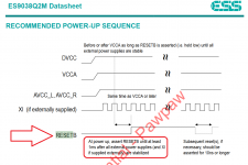
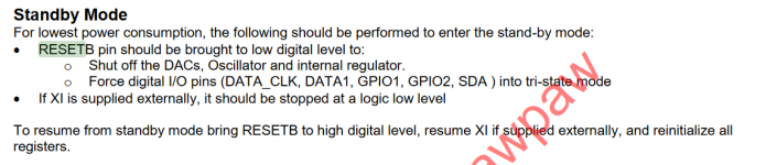
I design a 9038board but there are no output signal, does this chip need to enable some i2c register to turn on? When power on, i measure DVDD is 1.22V so the internal regulator is already turn on. Pin ResetB is also connect to 3.3V to turn the dac on.
I guess at least one register need to be set to get output.
Maybe more depending on input and settings.
I manage to get a Arduino to talk with the registers (with much help from Mark and others). Maybe that’s and option?
BR // Daniel
I guess at least one register need to be set to get output.
Maybe more depending on input and settings.
I manage to get a Arduino to talk with the registers (with much help from Mark and others). Maybe that’s and option?
BR // Daniel
I can use arduino to program it but after reading the datasheet, i don't think there is any register to turn on the dac, also the es9018k2m working without the need to write to any register. I compare my board to other and don't think it miss anything

I can use arduino to program it but after reading the datasheet, i don't think there is any register to turn on the dac, also the es9018k2m working without the need to write to any register. I compare my board to other and don't think it miss anything
Did you hardwire the reset pin without any reset circuit? (Did you hardware with just a trace on the PCB?) Or are you able to assert the reset after the power up sequence as per the datasheet (see attached)?
If you did not hardwire the reset have you tried toggling it after power up? Can you try toggling the reset after your power up to set the default state?
What does your reset circuit look like?Pin ResetB is also connect to 3.3V to turn the dac on.
Attachments
Last edited:
I can use arduino to program it but after reading the datasheet, i don't think there is any register to turn on the dac, also the es9018k2m working without the need to write to any register. I compare my board to other and don't think it miss anything
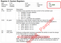
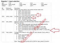
Are you inputting data as per the default settings of the input select resister?
What are you using as an input source? How do you know if it is or is not outputting data in the required default format?
Attachments
Hi proid,
This particular dac chip does need to be started up with an I2C register setting. Info about that in a few posts starting around #5607 of this thread. https://www.diyaudio.com/forums/digital-line-level/314935-es9038q2m-board-561.html#post6199036
If you have any other questions, please feel free to ask
- Home
- Source & Line
- Digital Line Level
- ES9038Q2M Board