C51 was gone. Pulled it out of the circuit and it is shorted (7.5R). Quite sure it was ok going in because I normally run those important caps over the LCR meter to make sure they match the filter values.
Polystyrene melts easily, that's why polystyrene capacitors are not used that often anymore. Pity, because they are very good capacitors.
Regarding the possibility of a 'bad' PCB, is SonnyMarrow's build using a PCB from the same manufacturing run? If so it suggests the PCB is OK as he has now has music, albeit still with some power supply issues to resolve.
acg checked an unpopulated PCB from the same batch and didn't find any shorts.
Different PCB's unfortunately. When I decided to do the project the Leadbelly boards were all spoken for (he found some extras though when he opened the box to mail them out) but I had my own batch made in the interim.
The bare pcb's here do not have the 'shorting' problem so I would be a little surprised if they end up being the problem.
The bare pcb's here do not have the 'shorting' problem so I would be a little surprised if they end up being the problem.
The orientations of all the ICs on the photo look fine to me. Any chance that you had the orientation wrong while measuring? That is, that everything is OK on the PCB, but pin numbers got mixed up while measuring?
I doubt it. The problem pins are the consecutive four that run under the throughhole IC to the left of the FPGA connector in the photo. J5.13 is the top one of those, J5.14/15/16 below. Touch two of these traces with the DMM probes and it beeps.
Polystyrene melts easily, that's why polystyrene capacitors are not used that often anymore. Pity, because they are very good capacitors.
Can't replace the failed cap until they get stock in July. May have to find an alternative should anybody have any sources for 10,000pF/10nF units.
I doubt it. The problem pins are the consecutive four that run under the throughhole IC to the left of the FPGA connector in the photo. J5.13 is the top one of those, J5.14/15/16 below. Touch two of these traces with the DMM probes and it beeps.
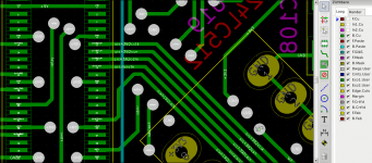
That matches exactly with what's in the KiCad database, so this also isn't it. See the attached picture, which is mirrored because KiCad displays the layout in top view and everything is on the bottom layer.
Attachments
Can't replace the failed cap until they get stock in July. May have to find an alternative should anybody have any sources for 10,000pF/10nF units.
I may still have one in the attic I'm not using.
There are usually a few polystyrene caps available from ebay sellers - that's normally where I pick mine up.
Surface traces can always be cut to ring out sections separately. Easy to solder back together afterwards.
Good point. If we dare to assume that the shorts on both PCBs (the damaged first PCB and the present PCB) have the same cause, acg can cut the tracks of his old PCB to localize the shorts and won't even need to solder them back.
Another thing to check, that doesn't even require any cutting: if and only if the short is beneath the SRC4392, chances are that U9 pins 22 and 23 are also shorted to ground.
Another thing to check, that doesn't even require any cutting: if and only if the short is beneath the SRC4392, chances are that U9 pins 22 and 23 are also shorted to ground.
U9.21/22/23 are not shorted to ground on either board. Here are the resistances for each pin on that side of U9 to GND:
24 0.1R RSTN
23 1.1M n/c
22 0.72M n/c
21 1.1M CDIN
20 0.1R CCLK
19 1.1M CSN
18 0.1R GND
17 175R VDD1.8
16 0.1R GND
15 0.74M n/c
14 0.5M MUTE
13 0.1R GND
Note that previously I had given in post #1708:
J5.13/15/17/19 all have <0.3R resistances to their pairs on U9...
But J5.13 also makes the following connections:
-> U9.24 <0.3R
-> U9.23 no connection
-> U9.22 no connection
-> U9.21 no connection
-> U9.20 <0.3R
-> U9.19 <0.3R
-> U9.18 <0.3R
-> U9.17 175R
-> U9.16 <0.3R
-> U9.15 500R
-> U9.14 450R
-> U9.13 <0.3R
I've not had time to digest this but at first glance it seems as though U9.20/24 are the only pins incorrectly connected to ground.
In other news I tried removing a damaged SMT IC from another pcb with the hot air gun and managed to pull a trace. Some of the chips for the ValveDac are larger than the one I practiced on so I have been looking for different ways to get them off. Today, I'll go into town to see if the electronics shop has some Chip Quick low melt solder or equivalent. That stuff looks easy to use with a high chance of me being able to remove things without harm. An even bet the shop will have some, otherwise I will order online and wait for arrival.
If you haven't already done so, you could try putting some fresh, narrow desoldering braid (solder wick) on the suspected pins of J5 and heating it up with a soldering iron, hoping it will suck out any excess solder. I have in some cases been able to remove shorts I couldn't see that way. Although I never tried this, I can imagine it may help to put a little flux on the pins beforehand.
If this doesn't remove the shorts, you can do the same with the associated pins of U9.
A rather more desperate method that I learned from a former colleague of mine is to force a current of a few amperes through the short, hoping it will melt any excess solder before damaging the PCB traces. If you are going to try that, please try it on your old board first. Take a lab supply that can deliver a few amperes, set it to 1.5 V and as high a current limit as possible, connect the negative output to the ground plane via the sturdiest connection you can find, scratch of solder mask from the shorted traces and connect the positive lab supply terminal there, one trace at a time.
I hope the contact resistance to the trace won't burn out the trace at the place where you connect the positive terminal. Otherwise you would have to solder a wire to the place where you removed the solder mask and connect the supply to the wire before switching it on.
Today, I'll go into town to see if the electronics shop has some Chip Quik low melt solder or equivalent.
Interesting stuff. I had never heard of low-temperature solder meant for solder removal. There is even an ROHS compliant version of it.
Chip Quik works like magic, some kind of indium-based low-melting point solder. Have to clean it off pads and pins before re-soldering with real solder. Easy enough to wick it up off pads; getting it out from in between fine pitch IC pins can be difficult. If the IC isn't to be reused then no problem.
Last edited:
The solder wick has already been tried. Only thing I could try is to re-flood the area with solder and then hope the wick grabs it all back plus any problem bridges already in place.
No luck with the local Chip Quick stuff...hopefully it will come with the mail on Monday and I can remove the entire J5 connector from the pcb and test to see if the problem goes away. Funny that the problem is with both pcb's though...it is a little worrying.
No luck with the local Chip Quick stuff...hopefully it will come with the mail on Monday and I can remove the entire J5 connector from the pcb and test to see if the problem goes away. Funny that the problem is with both pcb's though...it is a little worrying.
Chip Quik is brilliant and dead easy to use.
I have removed lots of 48 pin LQFP with zero pcb track damage.
Buy Chip Quik SMD1 Removal Kit | Mektronics Australia
I have removed lots of 48 pin LQFP with zero pcb track damage.
Buy Chip Quik SMD1 Removal Kit | Mektronics Australia
@acg,
You might try putting on some fresh solder, then dab on some liquid rosin flux and leave it to dry. After that try wicking with Chemwick, or another high quality wick. While it will remove most solder, it wouldn't be enough to completely unsolder a QFP or similar package. However, a hot air gun used for heat shrink can do it. Heat is less controlled than a hot air solder station can do, but it still works for removal.
You might try putting on some fresh solder, then dab on some liquid rosin flux and leave it to dry. After that try wicking with Chemwick, or another high quality wick. While it will remove most solder, it wouldn't be enough to completely unsolder a QFP or similar package. However, a hot air gun used for heat shrink can do it. Heat is less controlled than a hot air solder station can do, but it still works for removal.
Last edited:
In this case, it is probably a short at an 80-pin, 0.5 mm pitch SMD connector of this type B2B Stecker Hirose fur TE0300/TE0630 Industrie Mikromodul | Trenz Electronic GmbH Online Shop (DE) , although it could also be at a TQFP-48 IC (SRC4392). Rumour has it that the connectors can melt, although I haven't seen that happening yet.
- Home
- Source & Line
- Digital Line Level
- Valve DAC from Linear Audio volume 13