Thank you for your comments, billshurv.
Re. your first concern: I disagree. We have a piece of metal (high thermal conductivity) embedded into a layer of epoxy with a much lower conductivity. In such a configuration, most of the heat will flow along the metal part, and I don't expect the 2D effects to be prominent. In other words, I expect the metal plate within the chip to be nearly isothermal.
Re. your second concern: I quite agree with you, but this is not the point in this discussion. I entered it because of the claims that the 2K/W figure can not be changed by altering the cooling surface geometry. And even in the case of the T package, clamping the tab will result in a lower die temperature, which should not be a bad thing.
Ditto for the third one: I have not discussed the operating point of the chip. The test my colleague made was to prove that dissipating 100W without frying the chip is possible, i.e. that improved cooling is possible by enclosing the chip within a metal block.
Regards,
Braca
It's been a while since I did thermo analysis so happy to be wrong, but inspection suggests heat will want to flow from back of die out to heatsink by shortest path and not go sideways unless that is a preferential thermal path, in which case you have other problems.
The operating point is vital to this discussion as we need to understand what output power is needed to even get to this state. If its a case that no sane person would run as other problems (SOA for example) cause an issue then its a moot discussion. The main problem we all have is using the TF pack for this.
Hello all,
Have been following this thread with interest. Ever since I wanted to build a couple of chip amps ( I have 2 PD kits: 3875 and 4780 waiting to be constructed), I have been reading about heat sinks. A few years ago I received a deal on some 3/8" thick aluminum and some 2" high x 1/4" thick x 7" long copper bar pieces. So my plans are to use the aluminum for the chassis and use the copper as a spreader. The chip would attach to the copper, copper to the aluminum, with appropriate pad and/or thermal paste. I am planning to do monoblocks with the 3875 chips, and a paralled 4780 with the 4780 chips in one enclosure. Each chip will have its own copper spreader. The bottom and top of the chassis will be wood.
Question: "With the full 3/8" aluminum chassis as a heatsink, do you think I need the full 7" of copper bar, or could I get by with maybe a 3.5" long piece of copper per chip. This question may not be answerable, but thought I would ask for help. My take on this is to build it and see what happens, as I have seen many DIY heat sinks for these chips are smaller than what I am proposing.
Idea: Thinking of drilling some various sized countersinked holes on both sides of the piece of aluminum that would have the copper spreader attached, in an attempt to enlarge the surface area and to aid in the convection of the heat to the ambient air. What do you think????
Myles
My Update my Dynaco 3886 'kit' gut & rebuild of a Geriatric Dyna ST120.
Using the simple stoopid 1/4" ali plate OEM Dynaco heatsinks .
Do not even get warm ... on ~70 V rails. I mean I can barely feel Any heat at all
Even when left on overnight...inadvertently, after an overserving of Wine🙂
Why is this an issue elsewhere?
Connect your Dynaco to a resistive load and crank it to 25-30 W output power (about half the max output power with ±35 V rails). Leave it for an hour. I'd be surprised if it hasn't tripped the over-temp protection.
Most people listen to music at a few watt max. At that operating point, the dissipated power is pretty low, which is why your Dynaco doesn't heat up.
You mention you left it on overnight. Presumably, the music wasn't playing loudly overnight, right... So the only power dissipated in the LM3886 is the idle dissipation. On ±35 V rails, the LM3886 dissipates around 3.5 W if my quick math is right. 50 mA @ 70 W. Give or take. Not much to write home about.
If you'd like to do the math, I suggest having a look on my Taming the LM3886 website. Specifically, the Thermal Design section and the Power Supply Design section would be interesting. You can find the math in just about any textbook that covers the Class AB output stage. I recommend Sedra/Smith. The latest edition is ridiculously priced. The older editions contain the math as well.
~Tom
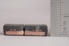
As promised the cross-section through the die, horizontally. That's the line C-C' in the diagram.
I had expected the copper DAP to be fragmented along this dimension, just as it is in the tab of the package. That wasn't the case, however. The copper goes all the way across the package. It ends about 1 mm from the edge of the package.
It's interesting to see how the leads are brought in, suspended above the DAP. It also looks like I just managed to nick a bond wire. Fun stuff...
It's too bad April 1st just went by. It would be fun to glue all the pieces together with super glue and start a "do you think my LM3886 is fake" thread... 🙂
~Tom
Attachments
Hi Tom,
Very interesting, thank's for sharing..
Maybe a Xray photograph would avoid destroying LM's 🙂
I think for 3875 and 3886, it's same case ?
Phil.
Very interesting, thank's for sharing..
Maybe a Xray photograph would avoid destroying LM's 🙂
I think for 3875 and 3886, it's same case ?
Phil.
It's been a while since I did thermo analysis so happy to be wrong, but inspection suggests heat will want to flow from back of die out to heatsink by shortest path and not go sideways unless that is a preferential thermal path, in which case you have other problems.
The operating point is vital to this discussion as we need to understand what output power is needed to even get to this state. If its a case that no sane person would run as other problems (SOA for example) cause an issue then its a moot discussion. The main problem we all have is using the TF pack for this.
The heat flow follows the shortest thermal path, i.e. the smallest thermal reistance, rather than the shortest distance.
Copper has a thermal conductivity of 400 W/(m x K), whereas the typical values for the epoxy resin used for IC packaging are between 0.3 and 1 (Intel quote 0.58-0.67 for the materials they use, and I've estimated the value of 0.3 for the LM3886 resin). So if we agree on 0.5 W/(m x K) as an average value, we see that the ratio of the conductivities in the copper plate and the resin is 1/800, which for me is a clear indicataion which path the heat flow takes.
An electrical analogue of this problem is a sereis connection of the resistive T-networks with low resistances (copper) in the horizontal direction, and high ones (epoxy) in the vertical direction. Driving the network with a constant voltage (i.e. temperature difference) I expect to see very low voltage (i.e. temperature) drop along the line, which is the same as the isothermal condition in the heat conduction case.
I agree with you on the operating point importance, but in my work I generally tend to identify the physical limits of the solution, whether meaningfull or not, an then to seek a meaningful variant in the solution space.
Regards,
Braca
I think you have missed what I was saying. Rapid sketch attached. Arrow shows direction I would expect max thermal gradient and therefore heat flow. To get out the top you effectively have 2 90 degree turns to make. If I had time I could test this by clamping a 3886 across the expoxy and cutting the tab off.
I could be wrong and happy for that to be the case here and it may be the 1D model works and you can assume equal heat flow from all metal surfaces (I use the T package)
I could be wrong and happy for that to be the case here and it may be the 1D model works and you can assume equal heat flow from all metal surfaces (I use the T package)
Attachments
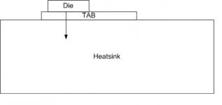
Bill, in your drawing there is a vital part missing. The 0.5mm epoxy between the tab and the heatsink (For the TF). Since the copper transfer heat 800 times better than epoxy it will have the same temperature along the whole structure.
Armand
Armand
No I haven't. I use the T package and I really question why anyone would want to push the limits with a TF. Makes no sense to me.
Totally agree.
But you must have some kind of electrical insulation between the LM3886 and the heat sink? And certainly that insulation will have far more thermal resistance than copper. So again I suspect that DNi's point is true.
It is another thing if the LM3886T's tab is directly connected to the heat sink. Even soldered as suggested here earlier.. How is your connected?
I have not decided yet. I was thinking of using a copper spreader, but when I get the rest of my parts will probably just use the stock silpad initially. Tom chides me for worrying too much but if you look at figure 33 of the LM3886 spec my ribbons are 3.1Ohms DC and so 50W looks to be about my limit. In which case I might as well get an 18VAC transformer and stop worrying about thermals. The speaker will be active so not like I will be short of volume. Ribbons are 83dB/2.83V (or 80dB/W) but inverse square law doesn't hold for a long source. Eventually suck it and see will kick in.
The heat flow follows the shortest thermal path, i.e. the smallest thermal reistance, rather than the shortest distance.
Copper has a thermal conductivity of 400 W/(m x K), whereas the typical values for the epoxy resin used for IC packaging are between 0.3 and 1 (Intel quote 0.58-0.67 for the materials they use, and I've estimated the value of 0.3 for the LM3886 resin). So if we agree on 0.5 W/(m x K) as an average value, we see that the ratio of the conductivities in the copper plate and the resin is 1/800, which for me is a clear indicataion which path the heat flow takes.
An electrical analogue of this problem is a sereis connection of the resistive T-networks with low resistances (copper) in the horizontal direction, and high ones (epoxy) in the vertical direction. Driving the network with a constant voltage (i.e. temperature difference) I expect to see very low voltage (i.e. temperature) drop along the line, which is the same as the isothermal condition in the heat conduction case.
We agree so far. Also as you pointed out, the copper will be isothermic (all the copper will be at the same temperature) as the thermal conductivity of the copper is much higher than that of the resin.
What is missing from your explanation above is how you calculate the thermal resistance from the copper DAP to the heat sink. If the LM3886 was sandwiched between two heat sinks, the thermal resistance to the back heat sink would be much lower than that to the front heat sink. No? Wouldn't this mean that the temperature gradient from the copper to the front of the package would be much greater?
~Tom
Maybe a Xray photograph would avoid destroying LM's 🙂
If you're willing to pay for the X-ray machine, I'll be happy to set it up... 🙂
I think for 3875 and 3886, it's same case ?
It's the same package, so odds are the package innards are identical. In some cases, you do see small tweaks to the lead frame due to a different lead frame vendor or different maximum die size requirements. Aside from allowing for a slightly different die size, these package tweaks don't change the performance of the package in any meaningful way. Not at audio frequencies. At >10 GHz it's a different story... 🙂
~Tom
We agree so far. Also as you pointed out, the copper will be isothermic (all the copper will be at the same temperature) as the thermal conductivity of the copper is much higher than that of the resin.
What is missing from your explanation above is how you calculate the thermal resistance from the copper DAP to the heat sink. If the LM3886 was sandwiched between two heat sinks, the thermal resistance to the back heat sink would be much lower than that to the front heat sink. No? Wouldn't this mean that the temperature gradient from the copper to the front of the package would be much greater?
~Tom
Thank you for your comments, Tom.
Your reasoning as to the LM3886 sandwiched between two heatsinks is correct. Since I need several lines of formulae and calculations to demonstrate my work, and the forum is text-based, I'll write a short note and post it as PDF document. So please bear with me until tomorrow.
I contacted the colleague who did the test posted here earlier by YU3MA, and he is willing to repeat it and have me present the data on this forum. I'm seeing him in three weeks' time, and depending on his schedule, the test should take place before the end of this month.
Regards,
Braca
Hello Dernofred,
The mounting tab will definitely soak more heat. You might like to have a look at the following one-dimensional heat conduction formula:
Q = k x A x DT / h
where:
Q - heat transfer rate [W],
k - thermal conductivity [W/m/K],
A - heat transfer area [sq. m],
DT - temperature difference [K],
h - material thickness between the die and the surface [m].
The expression K = h / (k x A) defines the thermal resistance in [K/W], in this case its value is 2 K/W.
Now increase the heat transfer area by clamping the front surface of the mounting tab to the heat sink by means of a piece of metal. If h and k are kept constant, which in the case of k is a reasonable assumption, and h is constant anyway, a 30% increase in the area reduces the thermal resistance by a factor of 1.3, i.e. to 1.54 K/W.
The above formula is all it takes to explain the increased heat transfer in the case of a chip enclosed in a metal block. Applying a more detailed theory, e.g. by considering the two-dimensional effects, would change the result by no more than a few percent in either direction.
Regards,
Braca
I agree in this view. It is like having fins in increase heat dissipation area or increasing airflow to carry the heat away. So what is really going on with adding heat sink around the chip is increating the dissipation speed.
The clamp design is something I envisioned as well.
Before the test is done it would be interesting to know what the output power was for this test. Slight stuck record, but no point wasting time if its for a unrealistic operating point that we would not even have been aware of were it not for YU3MA and his somewhat idiosyncratic agenda. Not least why the TF package. There must be a reason?
maybe higher back side resistance of tf makes this more worth than with t?? or it would be hard to isolate t version from all that cooper? 😕
I think they are exploring the limits of the chip. Unless you are thinking a about a hard rock home party, it would probably be rare for this limits to be reached.Before the test is done it would be interesting to know what the output power was for this test. Slight stuck record, but no point wasting time if its for a unrealistic operating point that we would not even have been aware of were it not for YU3MA and his somewhat idiosyncratic agenda. Not least why the TF package. There must be a reason?
Before the test is done it would be interesting to know what the output power was for this test. Slight stuck record, but no point wasting time if its for a unrealistic operating point that we would not even have been aware of were it not for YU3MA and his somewhat idiosyncratic agenda. Not least why the TF package. There must be a reason?
Yes, there was a reason, but before I begin with this subject I'd like to say that there was indeed a slight misunderstanding as to the 2D heat flow in the copper plate between the two of us, and I hope that it is settled now.
The colleague (I'm just reading his email) was asked to to repair a high power Sansui amplifier for which original spares were not available. The idea was to build a power stage replacement with 6 x LM3886 per channel in bridge configuration, and as he did not have the thermal resistance data for the plastic package, he decided to measure it. As a by-product of the experiment he also found out that the chips in his fixture can also sustain higher dissipation rates than suggested by TI. The chips in the block were wired as voltage regulators, and the output was a square wave feeding a resistive load.
I guess we could agree on the operating point for the new experiment.
Regards,
Braca
- Status
- Not open for further replies.
- Home
- Amplifiers
- Chip Amps
- LM3886 Thermal Experiment (with data)