Volume bump seems to be a race condition between set*SH_Range and set*SH commands. IF they are not executed at same exact moment, you will have a bigger or smaller volume drop or spike, depending on volume direction:
setLSE_Range(HIGH); setRSE_Range(HIGH);
setLSE(dataL.pw_SE); setRSE(dataR.pw_SE);
setLSH(dataL.pw_SH); setRSH(dataR.pw_SH);
goLowL = dataL.i_SH >= 32768 && LSHrange == HIGH;
goLowR = dataR.i_SH >= 32768 && RSHrange ==HIGH;
goHighL = dataL.i_SH < 32768 && LSHrange == LOW;
goHighR = dataR.i_SH < 32768 && RSHrange == LOW;
if (goLowL) setLSH_Range(LOW);
else if (goHighL) setLSH_Range(HIGH);
if (goLowR) setRSH_Range(LOW);
else if (goHighR) setRSH_Range(HIGH);
To minimize this effect and reduce the go* calculations delay, however small it might be, I moved the go* section to the top:
goLowL = dataL.i_SH >= 32768 && LSHrange == HIGH;
goLowR = dataR.i_SH >= 32768 && RSHrange ==HIGH;
goHighL = dataL.i_SH < 32768 && LSHrange == LOW;
goHighR = dataR.i_SH < 32768 && RSHrange == LOW
setLSE_Range(HIGH); setRSE_Range(HIGH);
setLSE(dataL.pw_SE); setRSE(dataR.pw_SE);
setLSH(dataL.pw_SH); setRSH(dataR.pw_SH);
// here is the critical delay
if (goLowL) setLSH_Range(LOW);
else if (goHighL) setLSH_Range(HIGH);
if (goLowR) setRSH_Range(LOW);
else if (goHighR) setRSH_Range(HIGH);
I also seem to have smaller volume bump with low ESR caps. To test the theory and increase the volume bump, put a delay (100) command instead of comment above.
Some people might get lucky and have these timings match perfectly, resulting in inaudible bump.
setLSE_Range(HIGH); setRSE_Range(HIGH);
setLSE(dataL.pw_SE); setRSE(dataR.pw_SE);
setLSH(dataL.pw_SH); setRSH(dataR.pw_SH);
goLowL = dataL.i_SH >= 32768 && LSHrange == HIGH;
goLowR = dataR.i_SH >= 32768 && RSHrange ==HIGH;
goHighL = dataL.i_SH < 32768 && LSHrange == LOW;
goHighR = dataR.i_SH < 32768 && RSHrange == LOW;
if (goLowL) setLSH_Range(LOW);
else if (goHighL) setLSH_Range(HIGH);
if (goLowR) setRSH_Range(LOW);
else if (goHighR) setRSH_Range(HIGH);
To minimize this effect and reduce the go* calculations delay, however small it might be, I moved the go* section to the top:
goLowL = dataL.i_SH >= 32768 && LSHrange == HIGH;
goLowR = dataR.i_SH >= 32768 && RSHrange ==HIGH;
goHighL = dataL.i_SH < 32768 && LSHrange == LOW;
goHighR = dataR.i_SH < 32768 && RSHrange == LOW
setLSE_Range(HIGH); setRSE_Range(HIGH);
setLSE(dataL.pw_SE); setRSE(dataR.pw_SE);
setLSH(dataL.pw_SH); setRSH(dataR.pw_SH);
// here is the critical delay
if (goLowL) setLSH_Range(LOW);
else if (goHighL) setLSH_Range(HIGH);
if (goLowR) setRSH_Range(LOW);
else if (goHighR) setRSH_Range(HIGH);
I also seem to have smaller volume bump with low ESR caps. To test the theory and increase the volume bump, put a delay (100) command instead of comment above.
Some people might get lucky and have these timings match perfectly, resulting in inaudible bump.
Last edited:
Don't think so cos I'm using the SR2's with Nebs code. For me the symptoms are at the 26-27 (out of 50) volume steps.
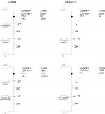
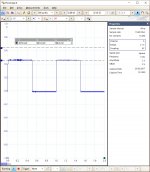
Attached are two scope traces. The Blue line is the voltage over R33 (RSH) and Red over R25 (RSE). The first screen grab is at vol 26 and the second at 27 where yoo can see the jump in RSH which results in the audible bump.
I'm currently using a tool called Meld to compare Nebs code with Vincents V1 code to see if there are any typos etc. I'll let you know if I find anything.
Thanks for posting this. The results are very interesting. I guess R33 and R25 are the current sense resistors on Neb's PCB? I think it would also be interesting to try and translate your findings into a transfer function for the current through the LDR as this is what really matters here?
Volume bump seems to be a race condition between set*SH_Range and set*SH commands. IF they are not executed at same exact moment, you will have a bigger or smaller volume drop or spike, depending on volume direction:
setLSE_Range(HIGH); setRSE_Range(HIGH);
setLSE(dataL.pw_SE); setRSE(dataR.pw_SE);
setLSH(dataL.pw_SH); setRSH(dataR.pw_SH);
goLowL = dataL.i_SH >= 32768 && LSHrange == HIGH;
goLowR = dataR.i_SH >= 32768 && RSHrange ==HIGH;
goHighL = dataL.i_SH < 32768 && LSHrange == LOW;
goHighR = dataR.i_SH < 32768 && RSHrange == LOW;
if (goLowL) setLSH_Range(LOW);
else if (goHighL) setLSH_Range(HIGH);
if (goLowR) setRSH_Range(LOW);
else if (goHighR) setRSH_Range(HIGH);
To minimize this effect and reduce the go* calculations delay, however small it might be, I moved the go* section to the top:
goLowL = dataL.i_SH >= 32768 && LSHrange == HIGH;
goLowR = dataR.i_SH >= 32768 && RSHrange ==HIGH;
goHighL = dataL.i_SH < 32768 && LSHrange == LOW;
goHighR = dataR.i_SH < 32768 && RSHrange == LOW
setLSE_Range(HIGH); setRSE_Range(HIGH);
setLSE(dataL.pw_SE); setRSE(dataR.pw_SE);
setLSH(dataL.pw_SH); setRSH(dataR.pw_SH);
// here is the critical delay
if (goLowL) setLSH_Range(LOW);
else if (goHighL) setLSH_Range(HIGH);
if (goLowR) setRSH_Range(LOW);
else if (goHighR) setRSH_Range(HIGH);
I also seem to have smaller volume bump with low ESR caps. To test the theory and increase the volume bump, put a delay (100) command instead of comment above.
Some people might get lucky and have these timings match perfectly, resulting in inaudible bump.
Nice find Neb! I guess the magnitude of the bump would also be dependent on the data* array which I guess is calculated during calibration and hence is differnet for each system?
Last edited:
My low-to-high bumps are gone. It was fiddly, but they are almost not audible any more, even with pink noise. I further optimized the code to have it set first left, then right channel:
setLSE_Range(HIGH); setRSE_Range(HIGH);
setLSE(dataL.pw_SE); setRSE(dataR.pw_SE);
////// LEFT
setLSH(dataL.pw_SH);
if (goLowL) {
delay(2);
setLSH_Range(LOW);
}
else if (goHighL) {
delay (6);
setLSH_Range(HIGH);
}
////// RIGHT
setRSH(dataR.pw_SH);
if (goLowR) {
delay(8);
setRSH_Range(LOW);
}
else if (goHighR) {
delay(4);
setRSH_Range(HIGH);
}
This is the part of the original code that was replaced:
setLSE_Range(HIGH); setRSE_Range(HIGH);
setLSE(dataL.pw_SE); setRSE(dataR.pw_SE);
setLSH(dataL.pw_SH); setRSH(dataR.pw_SH);
if (goLowL) setLSH_Range(LOW);
else if (goHighL) setLSH_Range(HIGH);
if (goLowR) setRSH_Range(LOW);
else if (goHighR) setRSH_Range(HIGH);
I had to fiddle with delays a lot.
setLSE_Range(HIGH); setRSE_Range(HIGH);
setLSE(dataL.pw_SE); setRSE(dataR.pw_SE);
////// LEFT
setLSH(dataL.pw_SH);
if (goLowL) {
delay(2);
setLSH_Range(LOW);
}
else if (goHighL) {
delay (6);
setLSH_Range(HIGH);
}
////// RIGHT
setRSH(dataR.pw_SH);
if (goLowR) {
delay(8);
setRSH_Range(LOW);
}
else if (goHighR) {
delay(4);
setRSH_Range(HIGH);
}
This is the part of the original code that was replaced:
setLSE_Range(HIGH); setRSE_Range(HIGH);
setLSE(dataL.pw_SE); setRSE(dataR.pw_SE);
setLSH(dataL.pw_SH); setRSH(dataR.pw_SH);
if (goLowL) setLSH_Range(LOW);
else if (goHighL) setLSH_Range(HIGH);
if (goLowR) setRSH_Range(LOW);
else if (goHighR) setRSH_Range(HIGH);
I had to fiddle with delays a lot.
Not sure what is different about my setup may be the caps but I used the ones specified in the oringinal BOM which are low ESR.
Nebs code did not help my setup. I have actually realised I have two bumps one in the right at the 26-27 transition and the other in the left at the 27-28 transition.
Playing around with the delays did not alter anything that I could tell other than how long it takes to rotate the volume control through that point.
Btw, I have one fully assembled and calibrated VxD All-In-One set for sale, OLED or LCD. PM me if interested.
Not sure what is different about my setup may be the caps but I used the ones specified in the oringinal BOM which are low ESR.
Nebs code did not help my setup. I have actually realised I have two bumps one in the right at the 26-27 transition and the other in the left at the 27-28 transition.
Playing around with the delays did not alter anything that I could tell other than how long it takes to rotate the volume control through that point.
I am taking back my low ESR statement, I have now the same bump size with generic caps and with low ESR ones. It's fairly small however.
I may have missed it but do we have any operational description of the circuit? Specifically the BIAS pins as it is this that triggers the bump
The click/bump is also there at 49-50 but I guess most people will never run their amps to the max.
There is also click evident when the mute relay clicks in. I was repeatedly using the encoder to go in and out of mute becasue there is a click there too. But it has all ended in tears... 🙁
All of the sudden the relay started to buzz and that is when I noticed the MCP23008 getting hot. Also guess which chips I decided not to socket! Time to order some spares. 😕
Last edited:
The click/bump is also there at 49-50 but I guess most people will never run their amps to the max.
There is also click evident when the mute relay clicks in. I was repeatedly using the encoder to go in and out of mute becasue there is a click there too. But it has all ended in tears... 🙁
All of the sudden the relay started to buzz and that is when I noticed the MCP23008 getting hot. Also guess which chips I decided not to socket! Time to order some spares. 😕
49-50 is not the same type of bump - there is just a non-linearity due to switching from calibrated resistance value to max-min one. Mute click is also yet another story - it's probably that you have a DC somewhere which loads/unloads the capacitance on connect/disconnect event.
I may be getting this all wrong as I'm reverse engineering, trying to understand what is going on. And at the moment my understanding is so messed up I cannot even see where a maximum current of 7mA can ever flow through any of the LDR LEDs?
If we take the Series LEDs, the datasheet specifies a forward voltage drop of 2.5V @ 20mA, but forgetting that for just a mo we have a 12V analogue supply & assuming Q1/2 are fully ON then that 12V supply is dropping through R7/24 & R9/26 (total 34K2). So if I have my ohms law correct that is a maximum current of 0.35mA excluding the voltage drop over the LED.
When the series sampling side is not being used the Nano sense lines get switched high (+5V) so I guess we have 7V/1K2 = 6mA (Close I guess)
The Shunt side is even more confusing because of the BIAS Pins D7/8 of the Nano and where the current sense signals are taken from given that thier resolution is over the 0-5V range. The max current through the LDR is 12V/35200R = 0.34mA.
When the shunt sampling side is not being used the Nano sense lines get switched high (+5V/Vol Bump) so I guess we have 7V/2K2 = 3.2mA
I MUST have this all wrong, but as I see it the issue is then not in the volume routines but the calibation?
Time for some breadboarding tests
When the series sampling side is not being used the Nano sense lines get switched high (+5V) so I guess we have 7V/1K2 = 6mA (Close I guess)
Hm, where do you see in the code sense lines (PIN_SENSE_*) being switched to output-high? I am also reverse-engineering it and could easily be wrong, but I can these pins being switched only between output mode and input mode:
/******* set high current/low resistance bias range *******/
// LOW = low resistance range
inline void setLSE_Range(byte val) {
pinMode(PIN_SENSE_LSE, val == LOW ? OUTPUT : INPUT);
}
inline void setRSE_Range(byte val) {
pinMode(PIN_SENSE_RSE, val == LOW ? OUTPUT : INPUT);
Unless it's a default value in output mode...
So attached are my breadboard tests. They make no allowence for the control via the transistor and show maximum LED currents/minimum LDR resistances for a given sample.
If I read the code right then some of the pins can be used to both read values and offer a 5V output.
On the shunt side if the BIAS pin goes high then the SENSE pin will see a voltage (V2) of over 5V which is outside of the AnalogRead range and could be suspect for the Nano itself
If I read the code right then some of the pins can be used to both read values and offer a 5V output.
On the shunt side if the BIAS pin goes high then the SENSE pin will see a voltage (V2) of over 5V which is outside of the AnalogRead range and could be suspect for the Nano itself
Attachments
Last edited:
Neb,
Forgive me I'm learning to code as I go so as well as trying to understand the project.
Looking at it again I think the default for a pin when changing its mode to OUTPUT is LOW which in that case makes it sink current effectively shorting out the 33K resistors so that means my previous tests were invalid. New tests attached
But it still leaves pins A6/7 exposed to high voltages if the shunts are driven to minimum resistance?
Forgive me I'm learning to code as I go so as well as trying to understand the project.
/******* set high current/low resistance bias range *******/
// LOW = low resistance range
inline void setLSE_Range(byte val) {
pinMode(PIN_SENSE_LSE, val == LOW ? OUTPUT : INPUT);
}
inline void setRSE_Range(byte val) {
pinMode(PIN_SENSE_RSE, val == LOW ? OUTPUT : INPUT);
Unless it's a default value in output mode...
Looking at it again I think the default for a pin when changing its mode to OUTPUT is LOW which in that case makes it sink current effectively shorting out the 33K resistors so that means my previous tests were invalid. New tests attached
But it still leaves pins A6/7 exposed to high voltages if the shunts are driven to minimum resistance?
Attachments
Regarding my other fault if I remove the Nano and just supply 5V to the board direct the MPC23008 chip still gets hot so that is blown. Which then got me thinking even more...
The A6/7 pins are next to the pins used for the i2C bus. Could they have got spiked by the possible overvoltages on A6/7. Cos the relay driver is still OK
All this thinking is getting out of hand
The A6/7 pins are next to the pins used for the i2C bus. Could they have got spiked by the possible overvoltages on A6/7. Cos the relay driver is still OK
All this thinking is getting out of hand
Nothing to apologize for, I am not programmer either - I learned a lot with this project😉
Anyway, if you are trying to get to the bottom of middle volume bumps, I don't think the calibration part is the culprit. People already measured resistance values on each step and they were spot on. The transition between steps while changing low-high resistance mode is the culprit, imho. There is no issue when they happen at exact same point in time, but sometimes they do not.
0-1 step click - probable issue with load RC network. I have this issue when I put VxD in front of gainclone, but not when I put it in front of another VxD, for example. You can disable mute function at vol=0 if you cannot weed it out at the source.
49-50 slight jump - this might be slight calibration issue. You can simply disable the last volume step if it bothers you:
else if (vol == VOL_MAX_STEP) {
setLSE_Range(LOW); setRSE_Range(LOW);
setLSH_Range(HIGH); setRSH_Range(HIGH);
setLSE(255); setRSE(255); setLSH(0); setRSH(0);
}
So I have replaced the damaged port expander and Nano (socketed this time) and I'm back online.
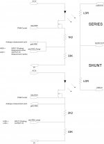
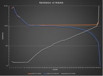
Attached is a basic drawing of the control signals and measurement points and what pins in the code they relate to. I have then gone through the 50 steps and mapped the values into a spreadsheet and plotted the results.
Not sure what it tells us fully yet but the bump at the middle and the top are a result of switching ranges. The schematic has also helped understand it a little better too.
Attachments
Last edited:
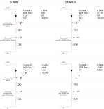
Here are some debugs while rotating encoder around range switching point:
Volume:31
RSH voltage:4057.20mV RSH current:0.12mA dataR:3323 RSHrange:1
Volume:30
RSH voltage:259.70mV RSH current:0.12mA dataR:32979 RSHrange:0
Volume:31
RSH voltage:4042.50mV RSH current:0.11mA dataR:3323 RSHrange:1
Volume:30
RSH voltage:274.40mV RSH current:0.12mA dataR:32979 RSHrange:0
30-31 transition bump I could cancel by delay, but 31-30 transition I could not - because falling edge and raising edge of two opposing events are not with the same slope. I cannot influence the shape of setRSH_range because it's done by switching pinmode from INPUT to OUTPUT LOW. But maybe I can do something about the other edge driven by PWM (dataR) so that slopes can cancel each other better.
Volume:31
RSH voltage:4057.20mV RSH current:0.12mA dataR:3323 RSHrange:1
Volume:30
RSH voltage:259.70mV RSH current:0.12mA dataR:32979 RSHrange:0
Volume:31
RSH voltage:4042.50mV RSH current:0.11mA dataR:3323 RSHrange:1
Volume:30
RSH voltage:274.40mV RSH current:0.12mA dataR:32979 RSHrange:0
30-31 transition bump I could cancel by delay, but 31-30 transition I could not - because falling edge and raising edge of two opposing events are not with the same slope. I cannot influence the shape of setRSH_range because it's done by switching pinmode from INPUT to OUTPUT LOW. But maybe I can do something about the other edge driven by PWM (dataR) so that slopes can cancel each other better.
My larger 2.42" display turned up today from Hong Kong so I was all excited. Wired it up... nothing. Noticed that all the surface mount components were hand soldered and all over the place. Then found an inductor with its terminals off angle to the pads and so it wasn't making connection. The componets must have been glued on first. Wired on some links and bingo it is all up and running!
If you look at the 26/27 crossover point on my table there does not seem to be a dramatic change in any of the resistances at least not out of step with the ones either side so as you say it must all be in the transition.
It is this same transition on the Series side at 49-50 that is responsible for the click there also. Of course that is easy to code out and in most instances will never be an issue anyway.
- Home
- Source & Line
- Analog Line Level
- Arduino based LDR volume and source selection controller